Key Statistics
Key Takeaways
- Market trajectory: SiC substrate sales are valued at USD 847 million in 2026 and projected to reach USD 3,762 million in 2036, implying 16.1% annualized growth through the ten-year forecast interval.
- Diameter transition: Six-inch substrates hold an estimated ~62% of 2026 value, while eight-inch wafers account for ~26% and show the strongest modeled expansion at ~22.9% CAGR; four-inch material retains a smaller legacy role.
- Demand concentration: Power components generate an estimated ~76% of 2026 demand, ahead of RF devices (~13%), optoelectronics (~7%) and other applications (~4%); automotive end users account for ~57% of the end-user lens.
- Geographic leadership: North America leads with an estimated ~34% share in 2026, followed closely by Asia-Pacific (~33%) and Europe (~25%); Chinese capacity additions and 200mm manufacturing are narrowing the regional gap.
- Commercial differentiator: Usable wafer yield, micropipe density, bow, warp and epitaxial compatibility matter more than gross crystal-growth capacity; 4H-SiC is modeled to supply ~83% of 2026 value.
- Investment catalyst: Wolfspeed expanded its commercial 200mm materials portfolio in September 2026, while Infineon and Wolfspeed signed a new 200mm wafer agreement in October 2026.
SiC Substrates Market Overview
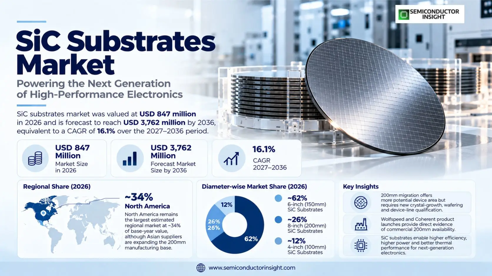
SiC substrates market was valued at USD 847 million in 2026 and is forecast to reach USD 3,762 million by 2036, equivalent to a CAGR of 16.1% over the 2027–2036 period. North America remains the largest estimated regional market at ~34% of base-year value, although Asian suppliers are expanding the 200mm manufacturing base.
Silicon-carbide substrates are engineered semiconductor wafers cut from SiC crystals and prepared for epitaxial growth or direct device processing. Their commercial value comes from crystal orientation, doping, resistivity, surface condition and defect control rather than wafer diameter alone. Compared with conventional silicon, 4H-SiC enables power devices to operate at high electric fields and temperatures, which can reduce conversion losses in automotive traction inverters, industrial drives and high-voltage infrastructure. Buyers qualify material against their own epitaxy and device-yield criteria.
The market boundary includes merchant and internally transferred SiC substrate wafers used for power components, radio-frequency devices, optoelectronics and the other applications represented in the segmentation. It includes conductive and semi-insulating grades, 4-inch, 6-inch and 8-inch diameters, and the 4H, 6H and 3C crystal-structure lens. It excludes finished MOSFETs, power modules, crystal-growth furnaces and separately sold epitaxial processing services. Bonded SiC substrates enter only when sold as substrate material within the defined application mix.
Wafer manufacturing starts with high-purity source material and controlled crystal growth, followed by boule inspection, slicing, edge grinding, lapping, polishing, cleaning and metrology. Defects including micropipes, basal-plane dislocations and stacking faults can propagate into epitaxial layers or compromise device reliability. Larger diameters offer more die area per wafer, but only if the manufacturer controls bow, warp, thickness variation and usable edge exclusion. Yield discipline therefore governs the economics of moving from 150mm to 200mm substrate production.
In September 2026 Wolfspeed introduced a premium 200mm n-type substrate intended to reduce defects and improve wafer-shape stability. Its stated micropipe specification of fewer than 0.01 per square centimetre illustrates the product-quality emphasis of the transition. Coherent has also expanded 200mm epitaxial-wafer manufacturing, while Resonac and Soitec are developing bonded 200mm material. These initiatives increase competitive pressure on conventional substrate suppliers to demonstrate consistent electrical and mechanical properties rather than relying on capacity announcements alone.
The 300mm opportunity requires separate interpretation. In January 2026 Wolfspeed reported producing a single-crystal 300mm SiC wafer, and Coherent began sampling high-thermal-conductivity 300mm substrates for AI infrastructure in August 2026. Those milestones concern emerging advanced-packaging and heat-spreading applications, not established 200mm power-device substrate volume. The quantitative model remains anchored to the published 4-inch, 6-inch and 8-inch classes; 300mm developments provide technology context without being added as an unreported sixth revenue category.
Segment Analysis: By Type
Diameter segmentation separates the established 150mm production base from the strategic 200mm migration. Six-inch wafers are modeled at ~62% of 2026 revenue, eight-inch at ~26%, and four-inch at ~12%. The larger format offers more potential device area but introduces new crystal-growth, wafering and device-line qualification requirements. Wolfspeed and Coherent product launches provide direct evidence of commercial 200mm availability.
| Diameter | Technical and manufacturing requirements | Commercial outlook |
|---|---|---|
| 4 Inch | 4 Inch SiC substrates require 100mm production tools and smaller specialty wafer lots. Material suppliers verify resistivity, orientation, micropipe density and edge quality before release. The customer must establish acceptable performance through 2 or more downstream operations such as epitaxy, implantation or device fabrication. The practical supply bottleneck is the number of qualified wafers that meet specifications, not the number of boules nominally grown. | 4 Inch represents an estimated ~12% of 2026 market value and is modeled to expand at ~5.5% annually through 2036. Demand is associated with legacy RF, optical and engineering programs. Purchasers consider cost per usable device area, contract stability and the ability to match multiple production lots. A diameter change can require a new substrate handling route and process-control baseline, making adoption dependent on customer investment timing. |
| 6 Inch | 6 Inch SiC substrates require 150mm crystal growth, slicing and well-established epitaxy recipes. For the 6 Inch substrate category, incoming-wafer acceptance depends on measured defect levels and consistent geometry over successive shipments. For the 6 Inch substrate category, process engineers validate the supplied crystal grade against the actual epitaxy and device recipe before authorizing repeat orders. For the 6 Inch substrate category, commercial availability must be evaluated through delivered qualified wafers rather than announced manufacturing nameplate capacity. | 6 Inch represents an estimated ~62% of 2026 market value and is modeled to expand at ~13.5% annually through 2036. Demand is associated with qualified automotive and industrial power-device supply chains. For the 6 Inch substrate category, contract pricing reflects yield risk, wafer diameter and the cost of requalification after a material specification changes. For the 6 Inch substrate category, purchasing decisions are influenced by wafer flatness, dislocation performance and the continuity of the supplier qualification record. |
| 8 Inch | 8 Inch SiC substrates require 200mm bow control, wafer flatness and lower-defect crystal quality. For the 8 Inch substrate category, production ramps become commercially significant only when customer inspection criteria are met on repeated manufacturing lots. For the 8 Inch substrate category, the receiving device line can reject material that falls outside its bow, resistivity or micropipe limits despite adequate nominal size. For the 8 Inch substrate category, yield at the substrate stage affects epitaxial utilization and the economics of subsequent high-voltage semiconductor fabrication. | 8 Inch represents an estimated ~26% of 2026 market value and is modeled to expand at ~22.9% annually through 2036. Demand is associated with large-volume power devices and next-generation fab conversions. For the 8 Inch substrate category, material selection links diameter, crystal polytype and finishing quality to the intended device and its manufacturing sequence. For the 8 Inch substrate category, a reliable supplier must coordinate delivery cadence with wafer-processing capacity and documented incoming-quality performance. |
Additional segmentation: End User and Crystal Structure
Two further segmentation dimensions explain demand without double-counting substrate revenue. Automotive end users are modeled at ~57%, telecommunications at ~16% and industrial buyers at ~27%. Crystal structure is concentrated in 4H-SiC at ~83%, with 6H-SiC ~12% and 3C-SiC ~5%. These modeled allocations describe different views of the same finished-wafer sales and reflect commercially established power-device material requirements.
| Additional axis | 2026 modeled distribution | Commercial interpretation |
|---|---|---|
| End User | Automotive ~57%; Telecommunications ~16%; Industrial ~27% | End User provides an additional allocation of the same substrate sales, not a separate market total. Automotive ~57%; Telecommunications ~16%; Industrial ~27%. The largest class is Automotive at ~57%. Commercial selection depends on the interaction between material characteristics and device use. End-user purchasing patterns reflect automotive, telecom and industrial qualification, while crystal-structure selection reflects polytype stability, electronic properties and manufacturing maturity. |
| Crystal Structure | 4H-SiC ~83%; 6H-SiC ~12%; 3C-SiC ~5% | Crystal Structure provides an additional allocation of the same substrate sales, not a separate market total. 4H-SiC ~83%; 6H-SiC ~12%; 3C-SiC ~5%. The largest class is 4H-SiC at ~83%. For the end-user and crystal-structure segmentation, incoming-wafer acceptance depends on measured defect levels and consistent geometry over successive shipments. Crystal-structure purchasing centers on 4H-SiC power-grade maturity, while 6H and 3C specifications remain tied to specialized research and optoelectronic uses. |
Segment Analysis: By Application
Power components are the dominant application for silicon-carbide substrates because electric vehicles, charging stations, solar inverters and industrial power systems benefit from efficient high-voltage switching. The modeled 2026 application mix assigns ~76% to power components, ~13% to RF devices, ~7% to optoelectronics and ~4% to other uses. Each application imposes different requirements for resistivity, polytype, surface finish and epitaxial compatibility.
| Application | Demand characteristics |
|---|---|
| Power Components | Power Components use conductive 4H-SiC for MOSFET and diode fabrication. This application is modeled at ~76% of 2026 revenue with a ~16.7% growth outlook through 2036. End-market exposure includes traction inverters, high-power chargers, renewable conversion and industrial drives. Material specifications are negotiated around conductivity, crystal orientation, defect density and lot-to-lot stability. Suppliers compete on usable wafer output and qualification support, because substrate price alone cannot capture the yield cost of defective downstream processing. |
| RF Devices | RF Devices use semi-insulating substrates for high-frequency transistor structures. This application is modeled at ~13% of 2026 revenue with a ~14.5% growth outlook through 2036. End-market exposure includes telecommunications infrastructure, radar and specialized RF electronics. For the rf devices application, process engineers validate the supplied crystal grade against the actual epitaxy and device recipe before authorizing repeat orders. For the rf devices application, commercial availability must be evaluated through delivered qualified wafers rather than announced manufacturing nameplate capacity. |
| Optoelectronic Devices | Optoelectronic Devices use optical and electronic material grades used in selected photonic structures. This application is modeled at ~7% of 2026 revenue with a ~13.5% growth outlook through 2036. End-market exposure includes specialty light emitters, optical devices and substrate-engineering research. For the optoelectronic devices application, contract pricing reflects yield risk, wafer diameter and the cost of requalification after a material specification changes. For the optoelectronic devices application, purchasing decisions are influenced by wafer flatness, dislocation performance and the continuity of the supplier qualification record. |
| Others | Others use research-grade and advanced materials outside the principal device groups. This application is modeled at ~4% of 2026 revenue with a ~11.5% growth outlook through 2036. End-market exposure includes new heat-spreading, packaging and experimental electronic applications. For the others application, production ramps become commercially significant only when customer inspection criteria are met on repeated manufacturing lots. For the others application, the receiving device line can reject material that falls outside its bow, resistivity or micropipe limits despite adequate nominal size. |
Commercial qualification is particularly demanding for automotive-grade power devices. A substrate change can affect epitaxial quality, transistor breakdown behavior and long-term reliability, so buyers generally validate incoming material across several process stages. RF customers prioritize semi-insulating characteristics and high-frequency performance, while optoelectronic and emerging packaging users may seek different thermal or optical properties. These requirements explain why one substrate supplier can be competitive in a niche without controlling the entire market.
Regional Analysis
North America leads the modeled 2026 regional distribution at ~34%, with Asia-Pacific close behind at ~33% and Europe at ~25%. Middle East & Africa contributes ~5% and South America ~3%. These shares allocate finished substrate revenue by commercial demand and supplier activity, not by the location of every finished electric vehicle or solar installation. Asia-Pacific is modeled to grow fastest at ~17.6% through 2036.
How does SiC substrate demand vary across manufacturing regions?
Crystal-growth expertise and qualified downstream fabs shape the geographic split. North American suppliers are active in large-diameter materials, European programs emphasize integrated automotive-grade supply, and Asian companies compete aggressively on scale and price. Emerging regions primarily purchase smaller volumes for specialized manufacturing or research. All five regional forecasts reflect the same global substrate revenue boundary, while modeled growth rates vary with 200mm adoption and local manufacturing readiness.
| Region | Position | Growth outlook | Demand profile | What decides supplier selection |
|---|---|---|---|---|
| North America | ~34% of 2026 market | ~15.8% CAGR | Commercial crystal-growth capability and materials r&d supports the regional demand profile. The commercial value depends on the share of qualified substrate manufacturing and purchases made by wafer-processing customers. The 2026 share is estimated at ~34% with growth of ~15.8% through 2036. For region table profile North America, customers compare crystal quality, downstream processing compatibility and supplier traceability before approving a recurring material specification. Changes in diameter or defect limits can trigger another qualification cycle, so announced capacity does not automatically become shippable substrate revenue. | High-yield 200mm qualification and predictable substrate delivery is the main supplier selection consideration in North America. Buyers inspect crystal defects, wafer flatness and delivery records before accepting a new source. Price competition is meaningful, but qualification and usable wafer yield determine repeat contracts across the 2027–2036 period. For region table gate North America, customers compare crystal quality, downstream processing compatibility and supplier traceability before approving a recurring material specification. For the North America supply channel, yield at the substrate stage affects epitaxial utilization and the economics of subsequent high-voltage semiconductor fabrication. |
| Asia-Pacific | ~33% of 2026 market | ~17.6% CAGR | Rapid scale-up in china, japan and south korea supports the regional demand profile. For the Asia-Pacific supply channel, material selection links diameter, crystal polytype and finishing quality to the intended device and its manufacturing sequence. The 2026 share is estimated at ~33% with growth of ~17.6% through 2036. For region table profile Asia-Pacific, customers compare crystal quality, downstream processing compatibility and supplier traceability before approving a recurring material specification. For the Asia-Pacific supply channel, a reliable supplier must coordinate delivery cadence with wafer-processing capacity and documented incoming-quality performance. | Competitive 150mm supply and low-defect 200mm ramp-up is the main supplier selection consideration in Asia-Pacific. For the Asia-Pacific supply channel, incoming-wafer acceptance depends on measured defect levels and consistent geometry over successive shipments. For the Asia-Pacific supply channel, process engineers validate the supplied crystal grade against the actual epitaxy and device recipe before authorizing repeat orders. For region table gate Asia-Pacific, customers compare crystal quality, downstream processing compatibility and supplier traceability before approving a recurring material specification. For the Asia-Pacific supply channel, commercial availability must be evaluated through delivered qualified wafers rather than announced manufacturing nameplate capacity. |
| Europe | ~25% of 2026 market | ~15.5% CAGR | Integrated automotive power-device ecosystems supports the regional demand profile. For the Europe supply channel, contract pricing reflects yield risk, wafer diameter and the cost of requalification after a material specification changes. The 2026 share is estimated at ~25% with growth of ~15.5% through 2036. For region table profile Europe, customers compare crystal quality, downstream processing compatibility and supplier traceability before approving a recurring material specification. For the Europe supply channel, purchasing decisions are influenced by wafer flatness, dislocation performance and the continuity of the supplier qualification record. | Automotive-grade reliability and multi-year qualification is the main supplier selection consideration in Europe. For the Europe supply channel, production ramps become commercially significant only when customer inspection criteria are met on repeated manufacturing lots. For the Europe supply channel, the receiving device line can reject material that falls outside its bow, resistivity or micropipe limits despite adequate nominal size. For region table gate Europe, customers compare crystal quality, downstream processing compatibility and supplier traceability before approving a recurring material specification. For the Europe supply channel, yield at the substrate stage affects epitaxial utilization and the economics of subsequent high-voltage semiconductor fabrication. |
| Middle East & Africa | ~5% of 2026 market | ~12.0% CAGR | Research and emerging power-electronics activity supports the regional demand profile. For the Middle East & Africa supply channel, material selection links diameter, crystal polytype and finishing quality to the intended device and its manufacturing sequence. The 2026 share is estimated at ~5% with growth of ~12.0% through 2036. For region table profile Middle East & Africa, customers compare crystal quality, downstream processing compatibility and supplier traceability before approving a recurring material specification. For the Middle East & Africa supply channel, a reliable supplier must coordinate delivery cadence with wafer-processing capacity and documented incoming-quality performance. | Specialist imports and technical-grade verification is the main supplier selection consideration in Middle East & Africa. For the Middle East & Africa supply channel, incoming-wafer acceptance depends on measured defect levels and consistent geometry over successive shipments. For the Middle East & Africa supply channel, process engineers validate the supplied crystal grade against the actual epitaxy and device recipe before authorizing repeat orders. For region table gate Middle East & Africa, customers compare crystal quality, downstream processing compatibility and supplier traceability before approving a recurring material specification. For the Middle East & Africa supply channel, commercial availability must be evaluated through delivered qualified wafers rather than announced manufacturing nameplate capacity. |
| South America | ~3% of 2026 market | ~11.0% CAGR | Limited direct wafer processing and import channels supports the regional demand profile. For the South America supply channel, contract pricing reflects yield risk, wafer diameter and the cost of requalification after a material specification changes. The 2026 share is estimated at ~3% with growth of ~11.0% through 2036. For region table profile South America, customers compare crystal quality, downstream processing compatibility and supplier traceability before approving a recurring material specification. For the South America supply channel, purchasing decisions are influenced by wafer flatness, dislocation performance and the continuity of the supplier qualification record. | Small-lot logistics and application-specific qualification is the main supplier selection consideration in South America. For the South America supply channel, production ramps become commercially significant only when customer inspection criteria are met on repeated manufacturing lots. For the South America supply channel, the receiving device line can reject material that falls outside its bow, resistivity or micropipe limits despite adequate nominal size. For region table gate South America, customers compare crystal quality, downstream processing compatibility and supplier traceability before approving a recurring material specification. For the South America supply channel, yield at the substrate stage affects epitaxial utilization and the economics of subsequent high-voltage semiconductor fabrication. |
Competitive Landscape
Competition is defined by crystal-growth yield, wafer quality and the ability to supply both 150mm and 200mm material under stable specifications. Wolfspeed and Coherent have direct commercial materials offerings, while TankeBlue, SICC, Resonac, ROHM-linked SiCrystal and other suppliers compete across geography and technical niches. The transition to larger diameters creates opportunities for differentiation through micropipe density, wafer shape and consistent epitaxial performance.
Wolfspeed commercialized a 200mm SiC materials portfolio in September 2025 and introduced a premium n-type 200mm substrate in September 2026. The latter emphasizes low micropipe density and wafer-shape stability. Those attributes address a practical customer concern: defects in the incoming substrate can undermine downstream epitaxy and reduce saleable power-device output. Its 2026 supply agreement with Infineon demonstrates commercial adoption of the larger diameter.
Coherent supplies SiC substrates and epitaxial wafers, with a 200mm product program and advanced thick-epitaxy capabilities. The company reported customer sampling of 300mm high-thermal-conductivity SiC material for AI infrastructure in August 2026, a separate emerging application from mainstream 200mm power-device wafers. Competitive advantage depends on combining crystal growth, wafering and process integration with reliable specifications across successive production lots.
Asia-Pacific suppliers compete through manufacturing scale, cost reductions and accelerated 8-inch qualification. TankeBlue and SICC are significant Chinese materials participants, while Resonac and Soitec are collaborating on bonded SiC substrates. The competitive challenge is to reduce cost per usable wafer without sacrificing defect density or flatness. Buyers may diversify sources, but switching requires validation of epitaxial and device reliability under the new material specification.
European integrated supply arrangements add another competitive dimension. ROHM subsidiary SiCrystal and STMicroelectronics extended a substrate supply agreement in April 2024, supporting long-term materials access for device manufacturing. The broader company list includes participants in devices, materials and related technology; inclusion does not establish that each has the same merchant-wafer revenue mix. Market positioning therefore should not be inferred from overall corporate semiconductor sales.
Tier structure
| Tier | Companies | Basis of competition |
|---|---|---|
| Tier 1 | Wolfspeed; Coherent | Commercial 150mm and 200mm substrate offerings, advanced materials engineering and direct product documentation support this group. Both companies have reported large-diameter manufacturing initiatives, but their product mixes and downstream relationships differ. Tier placement describes technical and commercial visibility rather than a verified ranking by revenue from this specific market boundary. For tier 1, customers compare crystal quality, downstream processing compatibility and supplier traceability before approving a recurring material specification. For the Tier 1 supplier tier, production ramps become commercially significant only when customer inspection criteria are met on repeated manufacturing lots. |
| Tier 2 | TankeBlue Semiconductor; SICC; Resonac; ROHM / SiCrystal; SK Siltron | These suppliers and materials programs participate in regional SiC crystal-growth and substrate supply. Their competitive roles include domestic capacity, bonded-wafer technology, automotive-grade qualification and customer diversification. Buyers assess wafer defect maps, conductivity, surface finish and the ability to sustain qualified deliveries as 200mm adoption expands over the forecast interval. For tier 2, customers compare crystal quality, downstream processing compatibility and supplier traceability before approving a recurring material specification. For the Tier 2 supplier tier, the receiving device line can reject material that falls outside its bow, resistivity or micropipe limits despite adequate nominal size. |
| Tier 3 | Beijing Cengol; Hebei Synlight; STMicroelectronics / Norstel; Dow; Nippon Steel; Ascatron; GeneSiC; SemiQ | This broader profiled group includes integrated manufacturers, materials specialists and device companies with varying exposure to substrate activity. Some participate primarily through internal wafer requirements or adjacent technologies rather than equivalent merchant-wafer sales. Individual revenue share cannot be inferred without product-level financial disclosures, so competitive comparisons should focus on documented capability and customer qualification. |
Key companies profiled
- Wolfspeed
- Coherent
- TankeBlue Semiconductor
- SICC
- Beijing Cengol
- Resonac
- Hebei Synlight
- STMicroelectronics / Norstel
- ROHM / SiCrystal
- SK Siltron
- Dow
- Nippon Steel
- Ascatron
- GeneSiC
- SemiQ
Production Capacity Analysis
Effective substrate capacity is the quantity of wafers that satisfy a customer’s specification after crystal growth, slicing, polishing and inspection. Nominal boule-growth output can overstate saleable supply when defects or shape variation cause rejection. The 150mm-to-200mm transition adds demands on thermal gradients, mechanical processing and metrology. Wolfspeed, Coherent and Asian materials suppliers are investing in this conversion while existing 6-inch production continues to serve qualified device lines.
Crystal-growth furnaces produce boules that are subsequently cut into wafers, but furnace count alone does not determine commercial output. The usable fraction depends on crystal defects, boule diameter, orientation and damage introduced during wafering. A 200mm wafer can provide more processing area than a 150mm wafer, yet yield losses can offset the nominal area advantage. Production planning therefore requires both process capability and downstream customer acceptance.
North America remains an important source of qualified large-diameter material through established producers, while Chinese suppliers are expanding commercial capacity and European programs integrate substrate supply with automotive power-device manufacturing. Cross-border shipments are common because crystal growth and device fabrication need not occur in the same country. Supplier diversification can reduce concentration risk, but a second source must reproduce electrical and mechanical specifications across many production lots.
Bonded-substrate approaches could alter future material productivity. Resonac and Soitec are developing 200mm bonded SiC substrates that use a thin single-crystal layer on a support wafer, potentially extracting more functional material from a donor crystal. The technology is not interchangeable with conventional bulk substrates for every application. Qualification, cost and device-process compatibility determine whether this route can capture significant 2027–2036 demand.
Market Dynamics
The strongest positive forces are the transition to 200mm production, demand for efficient power conversion and improvements in substrate yield. Restraints include crystal defects, manufacturing cost, price erosion and long automotive qualification cycles. The impact analysis assigns modeled percentage-point contributions to these forces for the 2027–2036 outlook, with stronger later-period influence from 200mm qualification and emerging high-voltage infrastructure.
MARKET DRIVERS
Drivers Impact Analysis*
| Market Drivers | Impact Rank | CAGR Contribution (%) | 2027–2029 | 2030–2032 | 2033–2036 |
|---|---|---|---|---|---|
| 200mm conversion in power-device fabs | High | +6.20% | High | High | High |
| EV and industrial power-electronics demand | High | +5.10% | High | High | Medium |
| Higher usable area and improved substrate yield | Medium-High | +4.00% | Medium | High | High |
| AI infrastructure and high-voltage power conversion | Medium | +2.70% | Medium | High | High |
| RF and specialty device diversification | Low-Medium | +2.00% | Medium | Medium | Medium |
| Others (supply localization, bonded-wafer innovation) | Low | +1.40% | Low | Medium | High |
200mm wafer conversion
Moving from 150mm to 200mm wafers can improve usable device area and process economics once crystal yield is controlled. Wolfspeed’s commercial 200mm products and Infineon’s 2026 supply agreement show that this transition has entered real procurement channels. The effect is not instantaneous: each device maker must qualify wafer bow, defect levels and epitaxy performance, so shipments follow customer process conversion.
Power electronics adoption
Automotive traction inverters, onboard chargers, solar conversion and industrial drives use SiC devices where high-voltage switching efficiency matters. Growth in these applications increases demand for conductive 4H-SiC substrate wafers. Material suppliers benefit when downstream device makers increase wafer starts, although inventory cycles and substrate price movements can make revenue more volatile than the underlying number of power devices produced.
Improved wafer yield
Better boule growth, lower micropipe density and tighter wafer-shape control raise the fraction of substrate output that customers can use. Wolfspeed’s September 2026 premium 200mm product illustrates the focus on material quality. Yield improvement can lower cost per usable die and encourage adoption of larger wafers, while suppliers must manage the resulting price pressure and investment requirements.
High-voltage infrastructure
AI data-center power systems, grid equipment and industrial conversion create additional demand for efficient high-voltage devices. Coherent’s April 2026 thick-epitaxy development for devices up to 10kV shows the technical direction of this market. Substrate revenue benefits only where these applications translate into qualified SiC wafer orders, not from the value of the finished power systems themselves.
MARKET RESTRAINTS
Restraints Impact Analysis*
| Market Restraints | Impact Rank | CAGR Contribution (%) | 2027–2029 | 2030–2032 | 2033–2036 |
|---|---|---|---|---|---|
| Crystal defects and costly 200mm yield ramp | High | -2.10% | High | High | Medium |
| Substrate price erosion and capacity oversupply | Medium-High | -1.50% | High | Medium | Low |
| Automotive qualification and demand volatility | Medium | -1.00% | High | Medium | Medium |
| Others (alternative materials, financing and logistics) | Low | -0.70% | Medium | Medium | Low |
Crystal-growth defects
Micropipes, dislocations and wafer-shape variation can reduce the usable output of SiC substrate manufacturing. Larger 200mm boules create more demanding thermal and mechanical conditions, so a capacity expansion may initially have a high rejection rate. Customers measure defects and epitaxial compatibility rather than accepting nominal diameter as proof of performance, delaying revenue from newly installed crystal-growth assets.
Price and oversupply pressure
Substrate suppliers face pricing pressure when 150mm capacity expands faster than qualified device demand. Higher yields can reduce unit costs, but competitive price reductions may offset shipment growth in revenue terms. Producers therefore need to differentiate through defect performance, wafer uniformity and reliable 200mm supply rather than relying solely on volume expansion. Contract structures and inventory cycles can also influence realized selling prices.
Automotive qualification cycles
Automotive power semiconductors require consistent performance over extended operating lives, making substrate-source changes technically sensitive. A new wafer specification can affect epitaxial defect levels, device reliability and production yield. Qualification may span multiple lots and process steps, delaying orders after a supplier announces a new diameter or premium grade. This favors proven supply relationships but also slows diversification.
Technology and funding risk
Advanced wafering and bonded-substrate approaches require equipment investment, intellectual property and reliable process transfer. Financing constraints can delay new crystal-growth capacity, while emerging 300mm applications remain at the development or sampling stage. Customers also compare SiC with silicon or gallium-nitride solutions at the device level, which can influence long-term demand without eliminating the specialized substrate requirement in qualified SiC processes.
MARKET OPPORTUNITIES
Premium low-defect 200mm wafers
Suppliers that reduce micropipes, threading dislocations and wafer-shape variation can sell higher-value substrates to device makers seeking better epitaxial yield. Wolfspeed’s September 2026 premium offering provides an example of a quality-led product strategy. The opportunity depends on repeatable inspection results and customer process acceptance, not simply on a claim that larger wafers are available.
Bonded substrate commercialization
The Resonac–Soitec 200mm program explores transferring a thin SiC crystal layer onto a support wafer, potentially using scarce single-crystal material more efficiently. If device makers qualify the resulting structure, suppliers could compete on cost per functional wafer and materials reuse. Commercial success remains conditional on reliability, interface quality and compatibility with epitaxial and device processes.
Diversified 200mm sourcing
Infineon’s October 2026 agreement with Wolfspeed illustrates demand for multiple qualified sources of large-diameter SiC material. Suppliers able to meet common defect and geometry specifications may win long-duration contracts as device makers reduce dependence on a single producer. The qualification barrier is substantial, but a successful second-source program can support stable deliveries and predictable capacity utilization.
Emerging thermal and AI applications
Coherent began sampling 300mm high-thermal-conductivity SiC substrates for AI infrastructure in August 2026, while Wolfspeed reported a 300mm single-crystal milestone in January. These initiatives could open packaging and heat-spreading applications beyond conventional power-device wafers. They remain emerging technical opportunities and should not be treated as established volume within the 4-inch, 6-inch and 8-inch forecast allocations.
Supply Chain Analysis
The SiC substrate value chain starts with purified source materials and crystal growth, then moves through boule slicing, wafer shaping, polishing, inspection and shipment to epitaxy or device manufacturers. The highest barriers are low-defect crystal growth and repeatable wafer finishing. Commercial demand is influenced by customer qualification and multi-year supply agreements, while automotive, RF and industrial users impose distinct electrical and reliability requirements.
Upstream. Crystal growth requires high-purity input materials and carefully controlled temperature gradients over long production cycles. Doping determines whether a substrate is conductive or semi-insulating, while polytype and orientation influence device compatibility. Material supply can become a bottleneck when producers move to larger boules, because furnace productivity and defect performance must improve together to generate saleable 200mm wafers.
Manufacturing. After growth, boules are sliced and processed into wafers with tightly controlled thickness, bow, warp and surface roughness. Each step can introduce damage or reject material, so the final yield depends on the complete manufacturing route. Coherent and Wolfspeed have described vertically integrated capabilities that link crystal growth to wafer preparation and downstream technical support, helping customers assess material consistency.
Qualification. A device maker evaluates incoming SiC wafers through epitaxy, defect mapping and electrical or reliability tests before approving regular deliveries. Automotive customers may require particularly consistent performance across successive production lots. Multi-source procurement can improve resilience, but the second supplier must meet the same acceptance criteria. The Infineon–Wolfspeed agreement is an example of long-term commercial sourcing for 200mm material.
Downstream. Power components are modeled to absorb ~76% of 2026 substrate revenue, with RF devices at ~13%, optoelectronics at ~7% and other uses at ~4%. The substrate is an upstream input and should not be valued at the selling price of the finished transistor or power module. Downstream growth can raise wafer demand, but inventory, yield and substrate pricing determine the revenue captured by materials producers.
Recent Developments in the SiC Substrates Market
- 15 October 2026 Announced
Infineon and Wolfspeed signed an expanded multi-year agreement to supply 200mm SiC wafers, extending their earlier 150mm relationship. The agreement supports Infineon’s manufacturing transition and strengthens its multi-source procurement strategy. For substrate suppliers, this is evidence of commercial demand for qualified 200mm material, although the parties did not disclose the agreement’s total wafer value. Source - 27 September 2026 Launched
Wolfspeed announced commercial availability of a premium 200mm n-type SiC substrate with improved wafer-shape consistency and stated micropipe density below 0.01 per square centimetre. The product targets higher device yield and more predictable epitaxy performance. Its introduction demonstrates the market shift from simple diameter availability toward tighter quality specifications and repeatable customer qualification. For dev sept2026, customers compare crystal quality, downstream processing compatibility and supplier traceability before approving a recurring material specification. For the silicon-carbide devs analysis, yield at the substrate stage affects epitaxial utilization and the economics of subsequent high-voltage semiconductor fabrication. Source - 17 August 2026 Sampling
Coherent began customer sampling of 300mm high-thermal-conductivity SiC substrates for AI infrastructure and advanced packaging. The company positioned the material as a potential heat-spreading solution for increasingly power-dense processors. This is a development-stage application distinct from established 200mm power-device substrates, and sampling does not establish commercial volume sales within the current diameter segmentation. For dev aug2026, customers compare crystal quality, downstream processing compatibility and supplier traceability before approving a recurring material specification. For the silicon-carbide devs analysis, material selection links diameter, crystal polytype and finishing quality to the intended device and its manufacturing sequence. Source - 9 April 2026 Announced
Coherent reported advances in thick SiC epitaxy on 150mm and 200mm platforms, supporting power-device architectures up to 10kV. The development broadens the technical applications for qualified SiC substrates in high-voltage industrial systems and data-center power distribution. Substrate quality and epitaxial uniformity remain linked, but the announcement describes technical capability rather than a disclosed substrate revenue contract. Source - 13 January 2026 Demonstrated
Wolfspeed reported producing a single-crystal 300mm SiC wafer and described potential uses in AI, AR/VR and advanced power electronics. The milestone demonstrates progress in large-diameter crystal growth, while substantial work remains before broad volume adoption. The 2026 market model does not allocate a separate 12-inch commercial segment because the established product axes cover 4-inch, 6-inch and 8-inch substrates. Source - 10 September 2025 Launched
Wolfspeed commercially launched its 200mm SiC materials portfolio, making larger-diameter substrates and related materials available for customer qualification. The announcement advanced the transition from pilot capability toward broader manufacturing adoption. Device producers can obtain more potential die area per wafer, but economic gains depend on material yield, defect control and compatibility with the receiving fab’s equipment. Source - 26 September 2024 Announced
Coherent announced expanded 200mm n-type SiC epitaxial-wafer production, including substrate and epi-wafer shipments at 350-micron and 500-micron thickness. The company stated that 200mm processing can provide about 1.8 times the usable area of 150mm wafers. The development supports large-diameter power-device manufacturing but does not eliminate the need for low-defect crystal growth and customer qualification. Source - 24 September 2024 Agreed
Resonac and Soitec agreed to jointly develop 200mm bonded SiC substrates for power semiconductors. The approach combines high-quality single-crystal material with bonding technology intended to improve productivity and material utilization. It provides an alternative manufacturing pathway that may influence cost and supply resilience, subject to customer validation of the bonded structure in actual device processes. Source
REPORT SCOPE & SEGMENTATION
| Attribute | Details |
|---|---|
| Study Period | 2021–2036 |
| Base Year | 2026 |
| Estimated Year | 2027 |
| Forecast Period | 2027–2036 |
| Historical Period | 2021–2025 |
| Market Size 2026 | USD 847 million |
| Market Size 2027 | USD 984 million |
| Market Size 2036 | USD 3,762 million |
| Growth Rate | CAGR of 16.1% from 2027–2036 |
| Unit | Revenue (USD Million) |
| Market Boundary | Bulk and bonded SiC substrate wafers for power, RF, optoelectronic and specified specialty applications; excludes finished devices, furnaces and separately billed services. |
| By Type | 4 Inch · 6 Inch · 8 Inch |
| By Application | Power Components · RF Devices · Optoelectronic Devices · Others |
| By End User | Automotive · Telecommunications · Industrial |
| By Crystal Structure | 4H-SiC · 6H-SiC · 3C-SiC |
| By Region | Five regional allocations for 2026–2036, with national manufacturing and procurement context. North AmericaUnited States, Canada, Mexico Asia-PacificChina, Japan, South Korea, Malaysia EuropeGermany, Italy, France, Austria Middle East & AfricaIsrael, United Arab Emirates, Saudi Arabia South AmericaBrazil, Argentina, Chile |
| Key Companies Profiled | Wolfspeed · Coherent · TankeBlue Semiconductor · SICC · Beijing Cengol · Resonac · Hebei Synlight · STMicroelectronics / Norstel · ROHM / SiCrystal · SK Siltron · Dow · Nippon Steel · Ascatron · GeneSiC · SemiQ |
| Customization Scope | Country-level wafer demand, 150mm-to-200mm qualification, application and polytype forecasts, and supplier-specific materials capabilities. |
Frequently Asked Questions
What is the SiC substrates market size in 2026?
The global SiC substrates market is valued at USD 847 million in 2026 and is projected to reach USD 3,762 million by 2036, implying 16.1% annualized growth across the forecast window. Revenue covers substrate wafers for power, RF, optoelectronic and other defined semiconductor uses. It excludes finished devices, complete process equipment and unrelated downstream system value.
Which region leads the SiC substrate industry?
North America holds the largest modeled 2026 share at ~34%, narrowly ahead of Asia-Pacific at ~33% and Europe at ~25%. Established materials producers and large-diameter technology programs support the North American position. Asia-Pacific is modeled to grow faster at ~17.6% annually, reflecting Chinese capacity additions and expanding device-manufacturing demand across several countries. For FAQ1, customers compare crystal quality, downstream processing compatibility and supplier traceability before approving a recurring material specification. For the silicon-carbide faq analysis, a reliable supplier must coordinate delivery cadence with wafer-processing capacity and documented incoming-quality performance.
What wafer diameter has the largest market share?
Six-inch SiC substrates account for an estimated ~62% of 2026 market revenue, compared with ~26% for eight-inch wafers and ~12% for four-inch products. The 150mm format remains a qualified production standard for many device lines. The 200mm class is modeled to grow fastest at ~22.9% annually, provided manufacturers improve crystal yield and customers qualify new equipment.
Which applications consume the most SiC substrates?
Power components are the leading application at an estimated ~76% of 2026 sales. RF devices account for ~13%, optoelectronics for ~7% and other specialized uses for ~4%. Automotive power conversion, industrial drives and renewable-energy electronics support demand for conductive 4H-SiC, while RF customers may require semi-insulating substrates with different resistivity and defect specifications. For FAQ3, customers compare crystal quality, downstream processing compatibility and supplier traceability before approving a recurring material specification. For the silicon-carbide faq analysis, incoming-wafer acceptance depends on measured defect levels and consistent geometry over successive shipments.
How important is the 4H-SiC crystal structure?
4H-SiC represents an estimated ~83% of the modeled 2026 substrate market, with 6H-SiC at ~12% and 3C-SiC at ~5%. The dominance of 4H-SiC reflects its established suitability for high-voltage power devices and many commercial substrate offerings. Other polytypes support specialized or developing applications, and the allocations describe material classes within the same revenue pool.
What drives adoption of 200mm SiC wafers?
The 200mm transition offers greater potential die area per processing cycle and can reduce cost per usable device when yields are controlled. Wolfspeed has commercialized 200mm material, and Infineon signed an expanded wafer supply agreement in October 2026. However, wafer bow, micropipe density, surface finish and epitaxial compatibility must meet customer standards before a larger diameter produces meaningful savings.
How does SiC substrate quality affect device yield?
Defects in the incoming substrate can propagate into epitaxial layers or contribute to device failures. Producers therefore measure micropipes, dislocations, wafer shape and surface condition before release. Wolfspeed’s September 2026 premium 200mm announcement illustrates the focus on defect reduction. A lower purchase price may not compensate for poor usable yield when a customer processes many wafers through expensive device-fabrication steps.
Who are major SiC substrate suppliers?
Wolfspeed and Coherent publish direct commercial SiC materials portfolios, while TankeBlue, SICC, Resonac, ROHM-linked SiCrystal and SK Siltron are important participants in the broader materials ecosystem. Additional companies have different degrees of merchant, captive or adjacent exposure. Supplier selection depends on qualified wafer specifications and delivery performance, not simply total corporate revenue or general semiconductor market position.
Are 300mm SiC substrates included in the forecast?
The published quantitative diameter classes are 4-inch, 6-inch and 8-inch, and those categories define the modeled market allocations. Wolfspeed’s January 2026 300mm single-crystal milestone and Coherent’s August 2026 300mm thermal-management sampling indicate emerging applications, but they do not establish a separately quantified commercial 12-inch category. Their potential is discussed as technology context rather than added to the base forecast.
What are the biggest risks to substrate market growth?
High crystal-growth costs, defects during diameter scaling, price erosion and lengthy automotive qualification can constrain revenue even when wafer shipments rise. Device makers may postpone equipment conversion or seek alternative suppliers after inventory adjustments. Producers that deliver low-defect 200mm material with stable lot quality and documented customer acceptance are better positioned to convert technical capacity into recurring commercial demand.
Research Sources & Evidence Base

Get Sample Report PDF for Exclusive Insights
Report Sample Includes
- Table of Contents
- List of Tables & Figures
- Charts, Research Methodology, and more...
 Download Sample Report PDF