Key Statistics
Key Takeaways
- Market outlook: the SiC wafer fabrication market reached USD 1,898 million in 2026 and is forecast at USD 9,856 million by 2036, representing 17.9% growth per year through the 2027–2036 outlook as 150 mm production matures and 200 mm fabrication gains customer qualification.
- Integrated device manufacturers: IDM manufacturing accounts for an estimated ~78% of 2026 activity, compared with ~22% for specialist foundries. The large integrated share reflects captive wafer-to-device flows, reliability qualification and control over epitaxy, lithography, implantation and packaging interfaces.
- Automotive power electronics: Automotive and EV/HEV represents an estimated ~45% of 2026 demand, followed by renewable generation and storage at ~19%, EV charging at ~14%, UPS and data-center power at ~13%, and other applications at ~9%.
- Geographic footprint: North America leads with an estimated ~36% of 2026 fabrication activity, followed by Asia-Pacific at ~32% and Europe at ~24%; the model assigns ~4% each to South America and Middle East and Africa, with qualification capacity concentrated in the first three regions.
- Execution risk: The move from 150 mm to 200 mm wafers increases potential die output but exposes manufacturers to crystal defect control, epitaxial uniformity, high-temperature process variability and slower automotive qualification; yield improvement rather than announced nameplate capacity determines realized revenue.
SiC Wafer Fabrication Market Overview
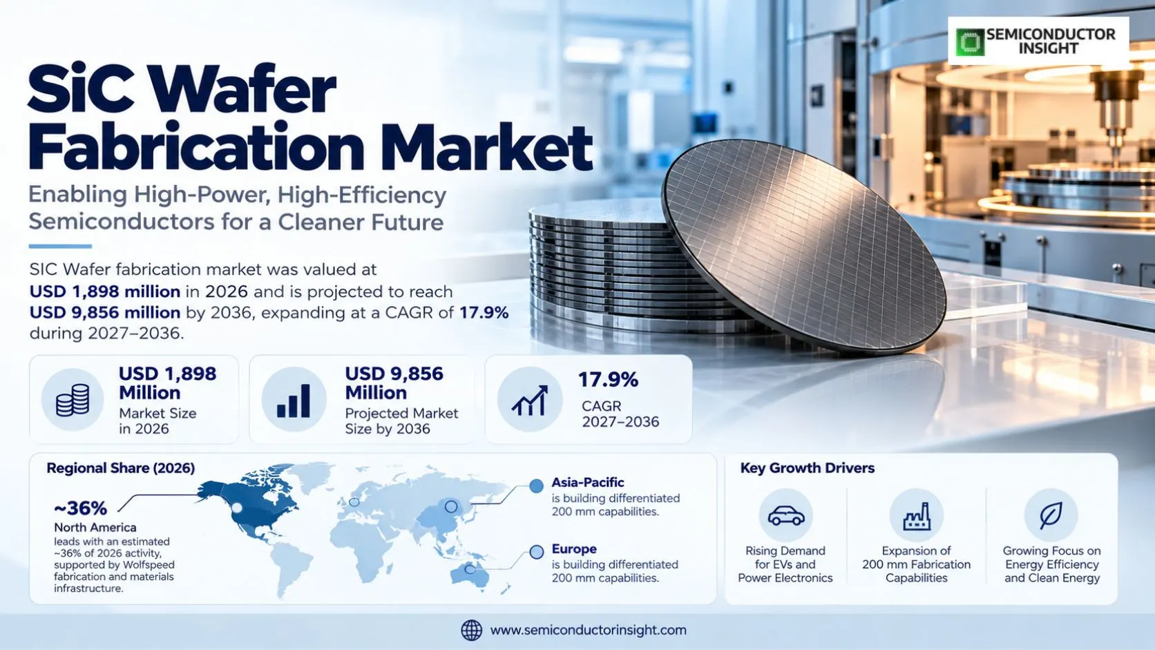
SIC Wafer fabrication market was valued at USD 1,898 million in 2026 and is projected to reach USD 9,856 million by 2036, expanding at a CAGR of 17.9% during 2027–2036. North America accounted for an estimated ~36% of 2026 activity, supported by Wolfspeed fabrication and materials infrastructure, while Asia-Pacific and Europe are building differentiated 200 mm capabilities.
Silicon carbide wafer fabrication combines crystal and substrate preparation, epitaxial growth and device front-end processing to manufacture power semiconductor wafers that withstand higher voltages and junction temperatures than conventional silicon. A finished wafer must pass material characterization, device patterning, implantation, activation, metallization and electrical testing before dicing or downstream module assembly. The manufacturing chain is capital intensive because SiC crystal quality and front-end process repeatability jointly determine usable die per wafer.
The market boundary encompasses the publisher-defined mix of integrated device manufacturer fabrication, specialist foundry services, wafer-supplier participation and strategic manufacturing alliances, with 150 mm and 200 mm production platforms. It includes activities associated with automotive inverters, charging, renewable-energy converters, industrial power systems and data-center power supplies. It excludes unrelated silicon CMOS fabrication, downstream vehicle sales and the entire revenue of diversified semiconductor companies; these activities are relevant demand signals rather than substitutes for SiC wafer fabrication value.
The transition from 6-inch, or 150 mm, substrates toward 8-inch, or 200 mm, processing is changing factory economics. Larger substrates offer more gross die sites per wafer, yet the benefit is not automatic: bow, thickness uniformity, basal-plane dislocations and edge exclusion can erode usable output. Wolfspeed commercially launched 200 mm bare wafers and epitaxy in September 2025, while Infineon released products manufactured with 200 mm SiC technology in February 2025, confirming separate material and device milestones.
Vehicle traction inverters are the principal demand connection because efficient 800 V powertrains and fast charging reward lower switching losses, smaller cooling systems and higher power density. The International Energy Agency documented expanding electric-car adoption in its 2025 outlook, although battery-electric vehicle sales do not translate one-for-one into wafer orders. Customer-specific device qualification, voltage class, packaging architecture and inventory adjustment can cause SiC fabrication revenue to diverge from the near-term trajectory of vehicle deliveries.
Manufacturing competition increasingly concerns the speed of a qualified process transfer rather than only construction of cleanroom capacity. STMicroelectronics announced a vertically integrated Catania SiC campus in May 2024, combining substrates, epitaxy, 200 mm front-end operations and packaging. Infineon inaugurated the first phase of its Kulim, Malaysia, SiC fab in August 2024. Both illustrate the multiyear interval between investment decisions, pilot production, customer acceptance and efficient high-volume output.
Segment Analysis: By Type
Two production models shape the SiC wafer fabrication market: IDM (Integrated Device Manufacturers) and Foundry. IDMs hold the largest estimated share, ~78% in 2026, while foundries represent ~22% and can expand through application-specific process development. Manufacturing strategy differs because integrated producers control chip specifications and final product responsibility, whereas foundries provide wafer process platforms for external designs.
| Type | Function | Market position |
|---|---|---|
| IDM (Integrated Device Manufacturers) | Integrated device manufacturers control wafer processing alongside chip design, reliability testing and frequently substrate or epitaxy sourcing. They align gate-oxide qualification, device layouts and high-temperature process recipes with the requirements of automotive and industrial power customers. This model can shorten feedback loops after field failures, although it ties capital spending to the manufacturer’s own product roadmap and factory utilization. | Largest type at an estimated ~78% in 2026; ~17.7% CAGR. Wolfspeed, STMicroelectronics and Infineon exemplify vertically coordinated SiC development and manufacturing. The model places the majority of revenue here because qualification accountability and process intellectual property favor integrated flows. Higher-volume 200 mm programs can reinforce this advantage if yield, line balance and downstream package capacity ramp together. |
| Foundry | Foundry fabrication provides process access for device developers that do not operate their own high-temperature SiC manufacturing lines. X-FAB introduced the XSICM03 platform in December 2024, with smaller cell pitch and a reusable process design framework intended to reduce custom MOSFET development risk. Foundries monetize process qualification, wafer runs and manufacturing services rather than relying exclusively on sales of proprietary finished power devices. | Estimated ~22% of 2026 value and ~18.7% CAGR. Specialist capacity is attractive when fabless customers need differentiated MOSFET structures without financing a dedicated factory. X-FAB’s December 2024 release cited cell-pitch reduction above 25% and a potential 30% increase in die per wafer relative to its prior platform. The commercial constraint is customer qualification volume, which may remain small during design-in periods. |
Secondary segmentation: End User
By end user, the leading class is Tier 1 Automotive Suppliers, accounting for an estimated ~46% of 2026 value. The other published members are Power Electronics Manufacturers, Renewable Energy System Providers. These categories distinguish who specifies device reliability, how much substrate diameter is available and which organizations bear wafer-process capital risk. The relative shares describe the publisher-defined SiC fabrication activity rather than total revenue of the companies operating in each category.
| End User members | Estimated commercial position |
|---|---|
| Tier 1 Automotive Suppliers | ~46% in 2026; ~18.8% CAGR |
| Power Electronics Manufacturers | ~37% in 2026; ~17.3% CAGR |
| Renewable Energy System Providers | ~17% in 2026; ~16.8% CAGR |
Secondary segmentation: Technology Node
By technology node, the leading class is 6-inch (150mm) Wafers, accounting for an estimated ~67% of 2026 value. The other published members are 8-inch (200mm) Wafers, Emerging Larger Formats. These categories distinguish who specifies device reliability, how much substrate diameter is available and which organizations bear wafer-process capital risk. The relative shares describe the publisher-defined SiC fabrication activity rather than total revenue of the companies operating in each category.
| Technology Node members | Estimated commercial position |
|---|---|
| 6-inch (150mm) Wafers | ~67% in 2026; ~16.6% CAGR |
| 8-inch (200mm) Wafers | ~29% in 2026; ~20.4% CAGR |
| Emerging Larger Formats | ~4% in 2026; ~19.4% CAGR |
Secondary segmentation: Business Model
By business model, the leading class is Device Manufacturer Verticals, accounting for an estimated ~59% of 2026 value. The other published members are Pure-play Wafer Suppliers, Strategic Alliances. These categories distinguish who specifies device reliability, how much substrate diameter is available and which organizations bear wafer-process capital risk. The relative shares describe the publisher-defined SiC fabrication activity rather than total revenue of the companies operating in each category.
| Business Model members | Estimated commercial position |
|---|---|
| Pure-play Wafer Suppliers | ~26% in 2026; ~18.5% CAGR |
| Device Manufacturer Verticals | ~59% in 2026; ~17.8% CAGR |
| Strategic Alliances | ~15% in 2026; ~17.0% CAGR |
Segment Analysis: By Application
The application split places Automotive & EV/HEV first at an estimated ~45% of 2026 fabrication value, with PV, Energy Storage, Wind Power at ~19%, EV Charging at ~14%, UPS, Data Center & Server at ~13%, and Others at ~9%. These modeled proportions reflect power-device adoption and production qualification, not the value of complete vehicles, charging stations or electrical infrastructure.
| Application | Demand characteristics |
|---|---|
| Automotive & EV/HEV | Vehicle traction inverters impose strict requirements for low conduction loss, temperature cycling and long-term reliability. Automakers evaluate 650 V, 750 V, 1,200 V and related SiC device classes according to battery architecture and drive-unit power. Wafer makers must therefore support automotive traceability and repeatable defect screening rather than only delivering low-cost substrates. Estimated share: ~45% in 2026, with a modeled ~18.6% CAGR through 2036. |
| EV Charging | High-power direct-current chargers require robust conversion stages and thermal management. SiC power devices can reduce passive component size and cooling load, but charging networks face utilization and capital-spending variability. Fabricators compete on switching performance, breakdown margin and supply continuity for 400 V and 800 V vehicle charging ecosystems. Estimated share: ~14% in 2026, with a modeled ~18.2% CAGR through 2036. |
| PV, Energy Storage, Wind Power | Renewable power systems use SiC in inverters, bidirectional converters and high-frequency power stages where efficiency matters over long duty cycles. Project procurement is sensitive to financing costs and grid connection schedules, so demand can move in batches. Wafer suppliers must demonstrate stable process control at the voltage and current ratings used in utility and commercial installations. Estimated share: ~19% in 2026, with a modeled ~17.4% CAGR through 2036. |
| UPS, Data Center & Server | Uninterruptible power systems and data-center power converters value high efficiency and power density as rack loads increase. Silicon carbide competes with silicon and gallium nitride according to converter topology and voltage class. Fabrication orders follow power supply platform qualifications, making reliability evidence and cost per usable die more important than headline computing-capacity forecasts. Estimated share: ~13% in 2026, with a modeled ~16.8% CAGR through 2036. |
| Others | Industrial drives, rail power conversion and specialized high-temperature electronics create smaller but diverse demand. These applications often require longer support periods and customized voltage or ruggedness specifications. Manufacturing partners can win durable programs through documented process change control, but qualification costs may be disproportionate when customer volumes remain below automotive production scale. Estimated share: ~9% in 2026, with a modeled ~16.6% CAGR through 2036. |
Sales channels differ between captive IDM wafer lines and foundry wafer-service contracts. Automotive Tier 1 suppliers frequently qualify a finished device or module with its manufacturing process locked down, whereas independent power-electronics manufacturers can negotiate wafer runs against design and reliability milestones. A 200 mm wafer transition may therefore increase potential output without immediately changing customer purchasing volumes or the pace of program nominations.
Regional Analysis
Regional fabrication activity is concentrated in North America (~36%), Asia-Pacific (~32%) and Europe (~24%) on the modeled 2026 basis, with Middle East & Africa and South America at ~4% each. North American SiC materials and device plants compete with Asian volume manufacturing and European vertically integrated investment. Each region has a different combination of factory capacity, customer proximity, public support and technical qualification.
How do fabrication footprints and qualification needs differ across regions?
North America concentrates important substrate and device manufacturing projects, with Wolfspeed’s 200 mm materials commercialization and Mohawk Valley device facility supporting customer access. Europe combines STMicroelectronics’ Catania plan and Infineon’s Villach capability, while Asia-Pacific includes Infineon’s Kulim investment and a broad power electronics customer base. These geographic positions are linked by cross-border wafer and module shipments, so local demand is not a direct proxy for factory output.
| Region | Position | Growth outlook | Demand profile | What decides supplier selection |
|---|---|---|---|---|
| North America | Largest (~36% share, 2026) | ~19.1% CAGR through 2036 | Integrated SiC manufacturing, materials development and vehicle inverter demand | automotive qualification, high-voltage device yield and domestic supply continuity |
| Asia-Pacific | Second largest (~32% share, 2026) | ~18.6% CAGR through 2036 | Automotive device manufacturing and Asian 200 mm factory ramp | factory scale, localized qualifications and 150 mm-to-200 mm process transfer |
| Europe | Third largest (~24% share, 2026) | ~15.9% CAGR through 2036 | Specialty power semiconductor fabrication and automotive qualification | European customer qualification, process traceability and integrated supply chains |
| Middle East & Africa | Specialty (~4% share, 2026) | ~15.5% CAGR through 2036 | Small local fabrication base and demand-led technology partnerships | import access, long service life and qualification of high-temperature power devices |
| South America | Specialty (~4% share, 2026) | ~14.8% CAGR through 2036 | Downstream industrial demand with limited indigenous SiC wafer capacity | distributor support, total installed-system cost and dependable replacement supply |
Key SiC Wafer Fabrication Manufacturers and Competitive Landscape
SiC fabrication combines a concentrated group of integrated power-device producers with a smaller specialty-foundry sector. STMicroelectronics, Infineon, Wolfspeed, ROHM and onsemi have meaningful device and manufacturing roles, while X-FAB offers a differentiated custom-process route. Competition depends on usable wafer yield, 200 mm transition execution, defect reduction, qualification records and customer confidence in long-term supply.
Integrated producers typically retain control over critical process recipes and device reliability data because a failed automotive traction inverter can trigger expensive investigation and replacement. Wolfspeed connects substrate materials with device manufacturing, while STMicroelectronics plans to integrate Catania substrate, epitaxy, front-end and back-end capabilities. These structures can improve traceability but create high fixed costs if the pace of SiC device adoption falls below the assumed factory ramp.
Infineon’s February 2025 product release from 200 mm technology in Villach illustrates that first customer shipments and full industrial scale are separate stages. The company also opened the first phase of its Kulim facility in August 2024. Production transfer between European and Asian sites depends on consistent process control, qualified equipment and equivalent reliability results; customers will not accept a new manufacturing origin solely because the wafer diameter is larger.
Specialist foundries provide a commercial alternative for smaller device designers. X-FAB launched its XSICM03 platform in December 2024, citing more than 25% smaller cell pitch and potential 30% higher die count per wafer than the previous platform. Those are company-specific platform comparisons, not industrywide manufacturing improvements. The economic attraction is reduced development overhead, while the challenge is filling production lines with stable customer programs.
Several profiled businesses participate through modules, power-device design, supply partnerships or upstream materials rather than operating independent SiC wafer foundries. Semikron Danfoss integrates power modules, while automotive Tier 1 companies specify qualification needs and may procure finished chips. Such ecosystem roles matter for the market’s commercial structure but should not be treated as proof that every named company operates a dedicated SiC wafer fabrication line.
Tier structure
| Tier | Companies | Basis of competition |
|---|---|---|
| Tier 1 integrated | STMicroelectronics, Infineon Technologies, Wolfspeed, ROHM Semiconductor, onsemi | Manufacturing platforms combining SiC device design, reliability engineering and proprietary front-end process control. These producers are positioned to serve automotive and industrial programs that require long product lifetimes, process change notifications and volume planning. Their challenge is to synchronize 150 mm output with 200 mm investments while limiting capital intensity and maintaining customer-approved electrical performance. |
| Tier 2 specialty and regional | X-FAB, BYD Semiconductor, San’an Optoelectronics, Mitsubishi Electric, Fuji Electric | Specialty manufacturing and regional power-device programs differentiate through customized device structures, local supply relationships and process engineering rather than only scale. X-FAB’s XSICM03 is a documented example of a customer-accessible SiC process platform. Customer qualification, wafer yield and device portfolio mix determine whether these capabilities translate into recurring production volumes across 2026–2036. |
| Module and ecosystem participants | Microchip Technology, Semikron Danfoss, Littelfuse, Toshiba, CETC 55 | These profiled participants influence SiC device demand through power electronics, modules, components, customer programs or regional ecosystems; their exact manufacturing roles differ. A supplier’s presence in a power-module catalog does not establish merchant SiC wafer-fabrication revenue. Selection for the table therefore distinguishes direct wafer processing capabilities from downstream purchasing and system integration that create demand for fabricated die. |
Key companies profiled
- STMicroelectronics
- Infineon Technologies
- Wolfspeed
- ROHM Semiconductor
- onsemi
- BYD Semiconductor
- Microchip Technology (Microsemi)
- Mitsubishi Electric (Vincotech)
- Semikron Danfoss
- Fuji Electric
- Toshiba Electronic Devices & Storage
- San’an Optoelectronics
- Littelfuse (IXYS)
- CETC 55
- X-FAB
SiC Wafer Fabrication Production Capacity Analysis
The global manufacturing base is transitioning from established 150 mm wafer flows to qualified 200 mm capacity. Wolfspeed’s North American infrastructure, STMicroelectronics’ Italian campus strategy and Infineon’s Austria–Malaysia network illustrate different approaches. Announced wafer starts and plant investment cannot be treated as current qualified output because crystal quality, epitaxy, device process steps and downstream testing must all meet customer limits.
Wolfspeed’s Mohawk Valley device facility opened in April 2022 and its Siler City materials operation reached a construction milestone in March 2024. The company commercially introduced 200 mm materials in September 2025, providing an important substrate qualification path for device makers. The material portfolio does not by itself establish finished device production at all customers; epitaxy uniformity, substrate defects and subsequent process integration remain separate constraints.
STMicroelectronics announced a multi-year investment program of around EUR 5 billion for Catania in May 2024, with Italian state support around EUR 2 billion and an eventual design capacity up to 15,000 wafers per week at full build-out. These are announced program parameters, not achieved 2026 output. The integration of substrates, epitaxy, front-end fabrication and packaging may reduce handoff friction if equipment qualification and utilization develop together.
Infineon inaugurated the first phase of Kulim’s 200 mm SiC facility in August 2024, with an initial investment volume of EUR 2 billion. Its February 2025 release of 200 mm-based products manufactured in Villach confirmed a commercial process milestone. The next constraint is matching process capability across sites while automotive customers validate production changes, particularly as factories shift from 150 mm equipment configurations toward 200 mm wafer handling and inspection.
SiC Wafer Fabrication Market Dynamics: Drivers, Restraints and Opportunities
Automotive inverter efficiency, renewable power conversion and 200 mm manufacturing investment drive SiC wafer fabrication growth. These positive forces compete with material defects, high-temperature process costs and slow customer qualification. The impact tables allocate percentage-point contributions to the modeled outlook and separate near-term execution risks from later-stage yield and adoption improvements.
MARKET DRIVERS
Drivers Impact Analysis*
| Market Drivers | Impact Rank | CAGR Contribution (%) | 2027–2029 | 2030–2032 | 2033–2036 |
|---|---|---|---|---|---|
| Automotive traction inverter platform adoption | High | +6.20% | High | High | Medium |
| 200 mm wafer process migration and yield gains | High | +5.40% | Medium | High | High |
| Industrial renewable-energy converter demand | Medium-High | +4.10% | Medium | High | High |
| Data-center and UPS power conversion upgrades | Medium | +3.40% | Medium | Medium | High |
| Specialty foundry and custom SiC process access | Low-Medium | +2.70% | Medium | High | High |
| Others (charging, rail traction, defense, high-temperature controls) | Low | +2.40% | Low | Medium | Medium |
Automotive power platform adoption
Battery-electric vehicle traction systems use SiC to reduce conversion losses and manage high voltage, particularly in 800 V architectures. The 2025 IEA Global EV Outlook documents substantial electric-car deployment, supporting long-run semiconductor demand. Fabrication suppliers must nevertheless win device and module qualifications that may precede volume shipments by years, making the automotive contribution sensitive to vehicle mix and design choices rather than simply unit sales.
Larger-diameter wafer economics
The industry’s 150 mm installed base supports current output while 200 mm programs seek more die per processed wafer. Wolfspeed launched a commercial 200 mm materials portfolio in September 2025, and Infineon began customer product releases from 200 mm technology in February 2025. These milestones improve technology availability, but die yield, equipment compatibility and process transfer determine the revenue benefit during the 2027–2036 forecast.
Renewable energy and industrial conversion
Solar, energy storage, industrial drives and rail systems use high-efficiency switching devices to reduce thermal losses and converter size. Silicon carbide fabrication demand increases when customers qualify MOSFET platforms for these applications, especially where high voltage and frequent switching favor SiC over silicon. Project financing and grid interconnection can postpone system orders, so wafer suppliers benefit from diversified customers and voltage classes rather than one end market.
Specialist foundry access and design diversity
X-FAB’s December 2024 XSICM03 announcement demonstrated how reusable SiC process blocks can reduce the development burden for customers seeking custom power MOSFETs. A smaller cell pitch and more die per wafer can improve economics when qualification targets are met. Foundry services extend the addressable design base beyond large integrated producers, although smaller customer programs may consume engineering capacity before producing sustained wafer volumes.
MARKET RESTRAINTS
Restraints Impact Analysis*
| Market Restraints | Impact Rank | CAGR Contribution (%) | 2027–2029 | 2030–2032 | 2033–2036 |
|---|---|---|---|---|---|
| Substrate defect density and gate-oxide yield | High | -2.30% | High | Medium | Medium |
| High-temperature process cost and utilization | Medium-High | -1.80% | High | High | Medium |
| Vehicle platform and customer qualification delays | Medium | -1.30% | Medium | Medium | Low |
| Others (power-device pricing, equipment lead times, inventory swings) | Low | -0.90% | Medium | Low | Medium |
Crystal defects and process yield
Silicon carbide substrate growth and epitaxy must control defects that can degrade breakdown voltage, leakage or device reliability. Higher processing temperatures and hard substrates make manufacturing more demanding than mainstream silicon wafer flows. Automotive qualification magnifies the cost of variation because traceability and long service-life evidence are required. A plant can therefore report 200 mm capability without achieving the same cost per qualified die as its mature 150 mm process.
Capital intensity and factory utilization
New wafer facilities require large commitments before customer demand is fully visible. STMicroelectronics announced a EUR 5 billion multi-year Catania program in May 2024, and Infineon described a EUR 2 billion first phase at Kulim in August 2024. Such figures represent announced investment scope, not realized sales. Underutilized equipment and costly process transfer can weaken economics even when demand for high-efficiency power electronics grows over the long term.
Customer qualification and platform timing
Automotive and industrial buyers often freeze manufacturing processes after validating reliability and electrical performance. Moving a device from 150 mm to 200 mm production can require renewed characterization, material traceability and process-change approval. A faster substrate roadmap does not automatically produce immediate vehicle program revenue. Inventory corrections, EV platform postponements and shifts between silicon, SiC and gallium nitride technologies can lengthen the interval between factory qualification and stable orders.
Competitive pricing and alternative technologies
Silicon carbide competes with improved silicon IGBTs and gallium nitride in different voltage and switching-frequency regimes. Customers may redesign converters to lower total system cost rather than adopt SiC in every power stage. Falling device prices can also offset wafer volume gains. Fabricators must therefore focus on defect reduction, process simplification and qualified product differentiation instead of assuming that 200 mm capacity alone ensures higher selling prices.
MARKET OPPORTUNITIES
200 mm ecosystem qualification
Materials suppliers and device fabs can coordinate wafer specifications, epitaxial thickness control, metrology and design rules as 200 mm platforms expand. Wolfspeed’s September 2025 commercial materials release and Infineon’s February 2025 device milestone demonstrate adjacent parts of this ecosystem. Suppliers that can document low defect variability and repeatable yields may gain access to customers migrating away from mature 150 mm manufacturing over the 2027–2036 window.
Custom MOSFET development services
Foundry customers increasingly seek tailored trench or planar MOSFET structures for specific switching-loss and reliability requirements. X-FAB’s XSICM03 process platform, launched in December 2024, supports a modular development route with documented process controls. This creates opportunities for design services, engineering wafer runs and eventually production contracts, particularly for companies without sufficient volume to justify a captive SiC fabrication line.
Regional supply resilience
The expansion of facilities in the United States, Italy, Austria and Malaysia offers customers more geographic sourcing options, although material supply and equipment dependencies remain global. Procurement teams can qualify multiple origins where process equivalence is demonstrated and inventory strategies justify the cost. Regional diversity is most valuable when the same device specifications, reliability limits and change-control practices can be maintained across manufacturing locations.
Power conversion in new infrastructure
Industrial electrification, grid storage, fast charging and high-density data-center power create additional demand beyond vehicle traction. Each application has different duty cycles, voltage classes and procurement rhythms, so broad qualification portfolios can stabilize wafer factory loading. Device makers that combine efficient high-voltage switching with robust packaging and traceable 150 mm or 200 mm wafer processes can address these opportunities without relying exclusively on automotive expansion.
SiC Wafer Fabrication Supply Chain Analysis
The SiC value chain links crystal growth and substrate finishing to epitaxy, front-end device fabrication, test, packaging and system qualification. 150 mm and 200 mm lines use overlapping materials but different equipment and handling constraints. Contractual risk is concentrated where wafer quality, process yield and downstream module acceptance interact, making manufacturing traceability an essential part of commercial supply.
Upstream materials. Substrate diameter and defect distribution establish the feasible yield envelope before a device fab starts processing. Wolfspeed’s 2025 commercial 200 mm materials introduction included bare wafers and epitaxy offerings, illustrating the importance of paired materials specifications. Crystal growth, slicing, polishing and epitaxy have different process bottlenecks; procurement teams therefore qualify both the wafer supplier and the compatibility of its materials with the downstream MOSFET process.
Front-end fabrication. Wafer processing adds epitaxial structures, patterned features, doped regions and contacts, with gate oxide quality particularly important for power MOSFET reliability. Transferring these steps from 150 mm to 200 mm changes thermal uniformity, equipment loading and inspection requirements. X-FAB’s XSICM03 announcement in December 2024 emphasized design rules and control plans, showing why stable process modules can be a competitive advantage for custom SiC customers.
Commercial channel. Integrated manufacturers may transfer wafers internally to device packaging and module lines, while foundries invoice engineering and wafer fabrication services to external designers. Wolfspeed’s long-term supply agreement with Renesas shows that materials contracts can extend across many years, reflecting the cost of qualification and the desire for predictable supply. The commercial boundary must therefore distinguish wafer fabrication activity from full downstream module or vehicle value.
End-use qualification. Automotive Tier 1 suppliers, power-electronics manufacturers and renewable-system providers test switching efficiency, breakdown behavior and thermal cycling at the finished-device or module level. Their approval depends partly on upstream wafer and process stability, even when they never purchase a bare SiC wafer directly. This indirect procurement structure explains why production qualification can lag equipment installation and why market demand should not be inferred solely from vehicle sales.
Recent Developments in SiC Wafer Fabrication
- 10 September 2025 Announced
Wolfspeed commercially launched its 200 mm SiC materials portfolio, including bare wafers and 200 mm epitaxy for customer qualification. The release described a 350 micrometre bare-wafer thickness and improved doping and epitaxial uniformity. This milestone expands access to larger-diameter materials but does not itself demonstrate finished-device yield at every downstream factory. Device makers must still qualify processing and reliability before the material transition contributes sustained high-volume revenue. Source - 13 February 2025 Announced
Infineon announced the first customer release of products made using its advanced 200 mm SiC wafer manufacturing technology at Villach, Austria, during the first quarter of 2025. It also described a planned 150 mm-to-200 mm transition at Kulim, Malaysia. The announcement establishes a device-level commercialization step distinct from substrate availability; later manufacturing economics will depend on volume ramp, yield and qualification across both facilities. Source - 17 December 2024 Announced
X-FAB introduced the XSICM03 SiC MOSFET process platform, reporting a cell pitch more than 25% smaller than its preceding generation and the potential for up to 30% more die per wafer. The manufacturer positioned the platform around modular process blocks and faster custom development. These comparisons apply to X-FAB’s specific technology generation rather than to all SiC foundries, and commercial adoption depends on customers completing device qualifications. Source - 8 August 2024 Announced
Infineon inaugurated the first phase of its SiC power semiconductor facility in Kulim, Malaysia, and described an initial EUR 2 billion investment volume. The 200 mm program aims to support high-efficiency devices used in vehicles, renewable energy and industrial conversion. Factory opening is a capacity-development milestone rather than evidence of immediate full utilization; yield improvement and customer commitments determine the pace at which the site converts installed equipment into saleable output. Source - 31 May 2024 Announced
STMicroelectronics announced a fully integrated SiC campus in Catania, Italy, linking substrate development, epitaxy, 200 mm front-end wafer fabrication, testing and module assembly. Its stated multi-year program involved around EUR 5 billion of investment and public support from Italy. The integrated structure is designed to shorten technical handoffs and improve traceability, but announced future wafer capacity should be distinguished from completed and customer-qualified production. Source - 25 April 2022 Announced
Wolfspeed announced the opening of its Mohawk Valley 200 mm silicon carbide fabrication facility in New York. The site represents a significant manufacturing commitment to higher-volume SiC power devices and a long qualification path for automotive and industrial customers. The opening date marks a factory milestone; the subsequent sequence of tool qualification, wafer starts, yield optimization and customer acceptance is what determines the amount of commercially usable device output. Source
REPORT SCOPE & SEGMENTATION
| Attribute | Details |
|---|---|
| Study Period | 2021–2036 |
| Base Year | 2026 |
| Estimated Year | 2027 |
| Forecast Period | 2027–2036 |
| Historical Period | 2021–2025 |
| Market Size 2026 | USD 1,898 million |
| Market Size 2027 | USD 2,238 million |
| Market Size 2036 | USD 9,856 million |
| Growth Rate | CAGR of 17.9% from 2027–2036 |
| Unit | USD million; wafer production and fabricated-device revenue context |
| Segmentation | By Type, By Application, By End User, By Technology Node, By Business Model and By Region |
| By Type | IDM (Integrated Device Manufacturers) · Foundry |
| By Application | Automotive & EV/HEV · EV Charging · PV, Energy Storage, Wind Power · UPS, Data Center & Server · Others |
| By End User | Tier 1 Automotive Suppliers · Power Electronics Manufacturers · Renewable Energy System Providers |
| By Technology Node | 6-inch (150mm) Wafers · 8-inch (200mm) Wafers · Emerging Larger Formats |
| By Business Model | Pure-play Wafer Suppliers · Device Manufacturer Verticals · Strategic Alliances |
| By Region | Five geographic regions analyzed by fabrication activity, type and application North AmericaUnited States, Canada, Mexico EuropeGermany, France, United Kingdom, Italy, Austria, other Europe Asia-PacificChina, Japan, South Korea, Malaysia, India, other Asia-Pacific South AmericaBrazil, Argentina, Chile, other South America Middle East & AfricaUnited Arab Emirates, Saudi Arabia, Israel, other Middle East and Africa |
| Key Companies Profiled | STMicroelectronics, Infineon Technologies, Wolfspeed, ROHM Semiconductor, onsemi, BYD Semiconductor, Microchip Technology (Microsemi), Mitsubishi Electric (Vincotech), Semikron Danfoss, Fuji Electric, Toshiba Electronic Devices & Storage, San’an Optoelectronics, Littelfuse (IXYS), CETC 55, X-FAB |
| Customization Scope | Custom country, customer, diameter, process and application splits available with purchase, subject to the agreed scope of analysis. |
Frequently Asked Questions
What is the SiC wafer fabrication market size?
The global SiC wafer fabrication market was valued at USD 1,898 million in 2026 and is projected to reach USD 9,856 million by 2036, with a CAGR of 17.9% over 2027–2036. The manufacturing scope includes integrated device maker wafer processing and foundry fabrication, with demand from traction inverters, charging, renewable conversion and industrial power electronics. The outlook assumes progressive 200 mm qualification alongside continued 150 mm output.
Which companies participate in SiC wafer fabrication?
The competitive landscape includes STMicroelectronics, Infineon, Wolfspeed, ROHM Semiconductor, onsemi, BYD Semiconductor and X-FAB, among other manufacturers and ecosystem participants. Their roles differ: some own integrated device and wafer process flows, some operate foundry platforms, and others focus on power modules or downstream device supply. Manufacturing claims should be checked against specific facilities and technologies rather than inferred from company-wide semiconductor revenue.
What does wafer fabrication include?
SiC wafer fabrication covers the steps that transform prepared silicon carbide substrates into patterned and tested semiconductor wafers. Epitaxy, lithography, ion implantation, high-temperature activation, gate formation, metallization and wafer-level electrical testing determine usable device output. The market also captures publisher-defined integrated and foundry manufacturing models, while excluding unrelated silicon CMOS fabrication and the entire value of downstream electric vehicles or power systems.
What are the main types of SiC wafer fabrication?
The two published types are IDM (Integrated Device Manufacturers) and Foundry. IDM production holds an estimated ~78% of 2026 value because many large power semiconductor companies integrate device design, wafer processing and reliability qualification. Foundries account for an estimated ~22% and offer custom process access to designers without captive fabrication. X-FAB’s December 2024 SiC MOSFET platform illustrates the foundry route for specialized power-device designs.
Which applications use fabricated SiC wafers?
Automotive and EV/HEV is the largest application, with an estimated ~45% share in 2026. Renewable generation and storage accounts for ~19%, EV charging ~14%, UPS and data-center power ~13%, and other industrial uses ~9%. These modeled shares describe wafer-fabrication activity associated with each end market, not the revenue of complete systems. Automotive qualification and converter architecture determine how quickly SiC adoption translates into production orders.
Which region leads SiC wafer fabrication?
North America leads the modeled 2026 allocation at ~36%, followed by Asia-Pacific at ~32% and Europe at ~24%. The remaining modeled ~8% is split between Middle East and Africa and South America. Wolfspeed’s U.S. materials and device investments support the North American position, while Infineon’s Kulim factory and European 200 mm programs illustrate competing capacity centers. Regional output and regional end-market demand are not identical.
Why is the industry moving from 150 mm to 200 mm wafers?
A 200 mm substrate provides more geometric area for devices than a 150 mm substrate, potentially reducing processing cost per qualified die when yields are comparable. Wolfspeed commercially released 200 mm materials in September 2025, and Infineon announced 200 mm-based customer products in February 2025. The transition still requires process transfer, defect management, tool qualification and customer approval, so economic benefits are not immediate or uniform across fabs.
What are the largest manufacturing restraints?
The principal restraints are substrate and epitaxial defects, high-temperature process cost, capital-intensive factories and customer qualification cycles. Automotive applications demand stringent long-term reliability and traceability, making changes in wafer diameter or fabrication location expensive to validate. Price pressure from silicon and gallium nitride alternatives can further limit revenue growth even as SiC device volumes rise. Factory utilization and usable die yield are therefore central operating metrics.
How do specialist foundries compete?
Foundries offer qualified SiC process flows to external designers that cannot justify building their own wafer factories. X-FAB’s XSICM03 platform, launched in December 2024, was designed to reduce development complexity and improve die density compared with its previous process generation. Foundries compete on process design kits, device reliability, customer engineering support and manufacturing flexibility, although smaller programs may require substantial qualification work before generating steady wafer volumes.
What is covered in the forecast and segmentation?
The study uses 2026 as the base year, 2027 as the estimated year and 2027–2036 as the forecast period, with historical coverage for 2021–2025. It analyzes IDM and foundry models, five applications, end-user classes, 150 mm and 200 mm technologies, business models and five global regions. Share estimates are modeled allocations grounded in disclosed factory and application evidence, while the monetary outlook follows the publisher’s headline endpoints.
Research Sources & Evidence Base
Get Sample Report PDF for Exclusive Insights
Report Sample Includes
- Table of Contents
- List of Tables & Figures
- Charts, Research Methodology, and more...
 Download Sample Report PDF