Key Statistics
Key Takeaways
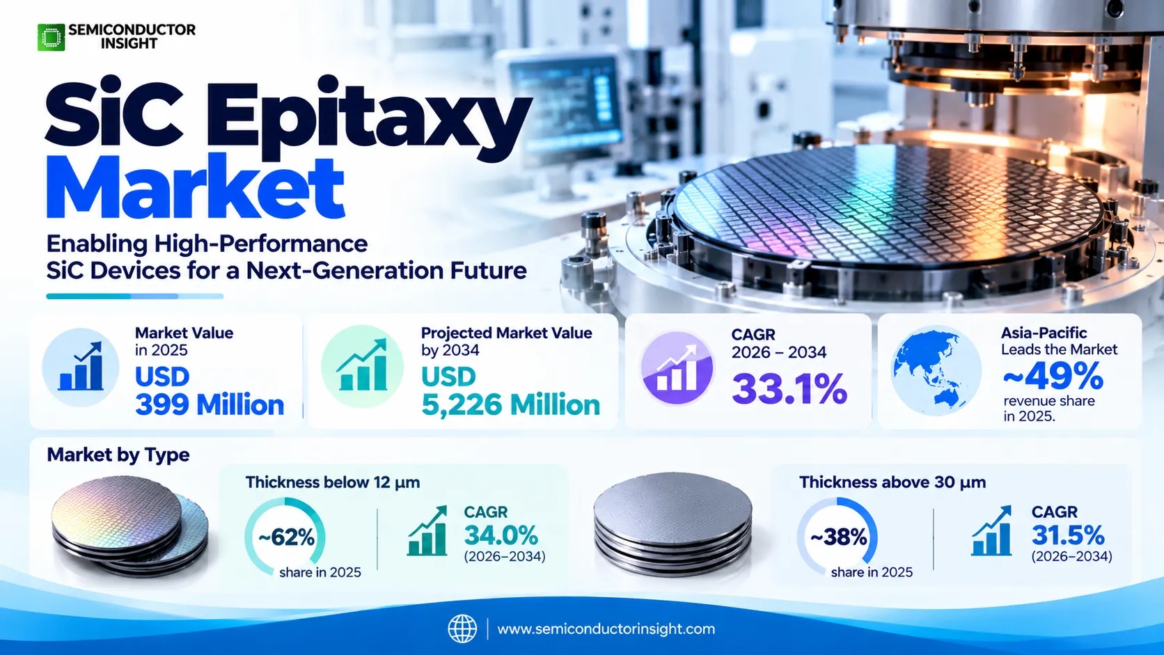
- Base-year demand: The global market was valued at USD 399 million in 2025 for silicon carbide epitaxial wafer material used in device fabrication.
- Forecast trajectory: Revenue is projected to reach USD 5,226 million by 2034 at a 33.1% CAGR during 2026–2034, reflecting wafer diameter transition and more demanding device structures.
- Leading type: Thickness below 12 µm represents an estimated ~62% of the modeled base-year mix, while layers above 30 µm account for ~38% of the named taxonomy.
- Type growth: The below-12 µm class grows at ~34.0% CAGR and the above-30 µm class at ~31.5% CAGR, supported by different device voltage requirements.
- Primary application: Power Component manufacturing contributes ~78% of estimated revenue, followed by RF Device at ~12% and Others at ~10%.
- Regional position: Asia-Pacific leads with ~49% of the modeled 2025 market; North America has ~22%, Europe ~19%, South America ~4%, and Middle East & Africa ~6%.
- Production shift: Commercial 200 mm epiwafers, uniform dopant profiles and lower defect densities are key to improved die economics and manufacturing qualification.
- Risk factors: Substrate crystal quality, epitaxial reactor productivity, thick-layer growth times and alternative semiconductor platforms constrain cost reduction.
Global SiC Epitaxy Market Overview
SiC epitaxy market was valued at USD 399 million in 2025 and is projected to reach USD 5,226 million by 2034, reflecting a 33.1% CAGR over 2026–2034. Asia-Pacific held the largest estimated 2025 share at ~49%, supported by SiC device fabrication and advanced wafer supply chains.
Silicon carbide epitaxy is the growth of a precisely controlled crystalline SiC layer on a compatible substrate wafer. The layer provides the doping profile, thickness and defect characteristics required for power semiconductor fabrication. The commercial boundary includes sold epitaxial wafers and the equivalent epitaxial-material value within integrated manufacturing, but not separately traded bare substrates, deposition equipment, completed MOSFETs, diodes or power modules. Epitaxial material is therefore upstream of devices and power-conversion systems, even when the same corporate group manufactures multiple stages.
Device yield depends on the quality of the epitaxial layer as much as the underlying crystal. Basal-plane dislocations, stacking faults, surface particles and dopant variation can degrade breakdown voltage and long-term reliability. Reactor gas flow, temperature control and precursor purity influence whether a wafer meets the customer’s specification. Qualification is demanding because small changes in crystal defects can propagate into downstream electrical failures, making stable process recipes and wafer-to-wafer repeatability valuable supplier capabilities.
The move from 150 mm to 200 mm diameter wafers is a major commercial transition. Larger wafers offer more usable device area per processing cycle, but the benefit is realized only if epitaxial uniformity and substrate quality remain consistent across the expanded surface. Coherent has described a 1.8-times usable-area advantage for 200 mm wafers compared with 150 mm formats, while Wolfspeed has made 200 mm epitaxy available for customer qualification. Manufacturing learning curves, not nominal reactor count alone, determine the pace of cost improvement.
The 2026 modeled market estimate is USD 531 million, with demand concentrated in power components for vehicle traction, renewable conversion and industrial switching. The Type split retains the publisher’s two labels, below 12 µm and above 30 µm, after correcting a corrupted micrometer character. No intermediate-thickness category has been invented. Thin layers serve many established device structures, whereas thicker and carefully doped epitaxial stacks are important for specialized high-voltage designs with different reactor-cycle economics.
Competitive positioning spans merchant epiwafer suppliers and vertically integrated device manufacturers. Coherent and Wolfspeed market SiC materials directly, while STMicroelectronics and Infineon combine material process development with device production. Resonac contributes epitaxial wafer technology in Japan. Former corporate names such as II-VI, Cree, Norstel and Showa Denko should be reconciled to their current owners, avoiding double counting and separating component demand from the sale of finished epitaxial material.
Segment Analysis: By Type
The published Type labels are Thickness below 12 µm and Thickness above 30 µm; the damaged unit symbol has been normalized to micrometers. The thinner class is modeled at ~62% of 2025 revenue and ~34.0% CAGR, while the thicker class accounts for ~38% with ~31.5% CAGR. These labels are preserved without fabricating a third category for the unlisted intermediate range.
| Type | Epitaxial growth requirements | Market position |
|---|---|---|
| Thickness below 12 µm | Thin epitaxial layers for routine power-device structures, where doping control and low surface defectivity support repeatable wafer processing. | Largest modeled type (~62% share; ~34.0% CAGR). Standard power-device fabrication favors short, uniform growth recipes that can achieve high reactor throughput. Device manufacturers still require tight control of dopant concentration and interface quality, because apparently small layer variations can reduce wafer yield. Production scale and repeatability are central to commercial success. |
| Thickness above 30 µm | Thick SiC layers for higher blocking-voltage devices and specialized industrial power applications with more demanding drift-region structures. | Specialized type (~38% share; ~31.5% CAGR). Longer deposition cycles raise reactor-time cost and increase the importance of defect management through the layer depth. High-voltage equipment can justify the expense when system performance depends on blocking capability, but qualification is rigorous and volumes are smaller than for common power devices. |
Thin-layer epiwafers and mainstream power electronics
Thin epitaxial layers support many SiC power devices where a controlled drift region and reliable junction formation are required. Suppliers optimize gas-phase chemistry, growth temperature and wafer handling to reduce contamination and nonuniformity. High reactor throughput is attractive only when electrical yield remains stable across batches. For automotive applications, a small defect population can create disproportionate warranty risk, so customers emphasize statistical process control rather than the nominal lowest cost per processed wafer.
The estimated ~62% share is a modeled commercial allocation based on broad power-device demand, not a measured breakdown of wafer shipments by micrometer thickness. Device manufacturers may use multiple epitaxial structures and buffer layers within a product family. Qualification of a new supplier therefore depends on the complete process specification, including dopant profiles and defect density, rather than on the thickness label alone.
Thick epitaxy for demanding blocking-voltage requirements
High-voltage power devices can require thicker, lower-doped epitaxial drift regions to achieve desired blocking performance. Growth time increases with layer thickness, making precursor utilization, thermal stability and reactor productivity economically important. Coherent has documented thick epitaxy supporting devices up to 10kV, illustrating a specialized technical direction. The segment may carry higher unit value per wafer, but high material cost and long qualification cycles restrain adoption in less demanding electrical systems.
Segment Analysis: By Application
Power Component fabrication dominates the application model with an estimated ~78% share and ~34.0% CAGR. RF Device contributes ~12% at ~29.0% CAGR, while Others accounts for ~10% at ~30.0% CAGR. Application shares represent epiwafer-material demand and do not include the selling prices of complete transistors, amplifiers, converters or vehicles.
| Application | Demand characteristics |
|---|---|
| Power Component | Primary application (~78% of 2025 revenue; ~34.0% CAGR). Epitaxial wafers supply SiC MOSFETs and diodes used in traction inverters, fast chargers, industrial drives and grid conversion. Customers require controlled drift-region thickness, dopant uniformity and low defect density because device breakdown behavior and switching reliability are sensitive to the material. Expansion to 200 mm increases the importance of within-wafer consistency. |
| RF Device | Specialty application (~12% share; ~29.0% CAGR). High-frequency and high-power device supply chains use compound semiconductor platforms with stringent material specifications. SiC can serve as a thermally robust platform or support specialized device structures, but RF product architecture differs from mainstream power MOSFET manufacturing. The modeled allocation therefore remains modest and should not be equated with the broader GaN-on-SiC RF market. |
| Others | Remaining application (~10% share; ~30.0% CAGR). Research devices, specialty sensors and experimental high-voltage structures require customized epitaxial thickness and doping profiles. Commercial volumes are smaller, and some orders are for engineering qualification rather than continuous production. Suppliers can differentiate through flexible recipes and defect control, although customer-specific specifications make the segment difficult to scale as a standardized commodity. |
Automotive power semiconductor demand is an important downstream influence but is not itself epitaxial wafer revenue. A single vehicle may contain several power devices fabricated on different wafer processes, and the epiwafer share of the finished system value is only one upstream input. The IEA reports more than 20 million electric cars sold globally in 2025, providing evidence of potential device demand rather than a direct measurement of epitaxy shipments.
Power-device manufacturers may integrate epitaxial growth inside their fabrication operations or buy epiwafers from specialist materials companies. Captive production and merchant sales have different accounting boundaries, so comparing supplier revenue requires attention to internal transfers. RF and specialty customers can pay for unusual specifications, but their qualification cycles and wafer volumes differ from the mass-production power market.
Regional Analysis
Asia-Pacific is the largest regional epiwafer market at an estimated ~49% share and ~35.0% CAGR, followed by North America at ~22% with ~31.0% CAGR and Europe at ~19% with ~32.0% CAGR. South America holds ~4% at ~29.0% CAGR and Middle East & Africa ~6% at ~29.3% CAGR. These are modeled commercial allocations, not audited manufacturing shipment shares.
Where is SiC epitaxial wafer manufacturing and demand concentrated?
Regional concentration follows the location of power semiconductor fabrication, substrate availability and specialist epitaxy expertise. China, Japan, South Korea and Southeast Asia form a dense manufacturing network, while North America retains important material technology and European manufacturers are investing in integrated SiC production. Smaller regions participate mainly through device demand and industrial power applications rather than large established epitaxy plants.
The location of an epiwafer growth reactor does not necessarily determine the location of the final customer. A material may be grown in one country, processed into devices in another and installed in power modules elsewhere. Regional shares therefore describe the modeled market opportunity, with differences in merchant sales, captive production and cross-border transfers explicitly recognized.
| Region | Position | Growth outlook | Demand profile | What decides supplier selection |
|---|---|---|---|---|
| Asia-Pacific | Largest (~49%) | Fastest (~35.0% CAGR) | Device fabs and material suppliers | Epiwafer defectivity, 200 mm transition and customer qualification |
| North America | Second (~22%) | Expansion (~31.0% CAGR) | Materials R&D and power devices | High-voltage specifications, quality systems and supply agreements |
| Europe | Third (~19%) | Industrial growth (~32.0% CAGR) | Integrated SiC manufacturing | Automotive qualification, local capacity and energy costs |
| South America | Small (~4%) | Emerging (~29.0% CAGR) | Downstream device demand | Import access, project timing and specialized engineering support |
| Middle East & Africa | Developing (~6%) | Selective (~29.3% CAGR) | Power infrastructure demand | Investment scale, reliable materials sourcing and training |
Global SiC Epitaxy Competitive Landscape
Competition is divided between merchant epiwafer materials suppliers and vertically integrated semiconductor producers. Coherent, Wolfspeed and Resonac offer differentiated material capabilities, while STMicroelectronics and Infineon combine epitaxial process requirements with their own device manufacturing. Historical names are consolidated under current owners to avoid presenting acquired operations as independent competitors, especially when reviewing long-running customer qualification records and technical product histories.
Merchant suppliers compete through defect density, thickness and doping uniformity, diameter capability and responsiveness to customized device structures. A customer changing epiwafer source must repeat electrical and reliability qualification, making long-term process consistency commercially important. Price remains relevant, but a lower wafer cost can be outweighed by losses in downstream die yield. Suppliers with stable material specifications can therefore defend relationships even when rivals offer larger nominal capacity.
Vertically integrated manufacturers have different economics because epitaxy can be performed inside the same corporate production system as device fabrication. Internal process knowledge enables rapid feedback from electrical test results to growth recipes, while captive material flows are not always visible in merchant market statistics. These manufacturers may buy substrates externally, perform epitaxy internally or source finished epiwafers according to technology and capacity constraints.
Coherent’s portfolio covers standard and thick epitaxial structures, including multilayer and junction options. Wolfspeed’s 200 mm materials launch makes epitaxy available for customer qualification, and Resonac has emphasized high-grade material with reduced defect populations. The supplier comparison should focus on published technical capabilities and commercial availability rather than assumed company market shares, because detailed comparable epitaxy-only revenue is not consistently disclosed.
Several legacy company labels require reconciliation. II-VI Advanced Materials now falls under Coherent, Cree materials operations are associated with Wolfspeed, Norstel became part of STMicroelectronics, and Showa Denko is now Resonac. Those names can remain useful when interpreting historical specifications, but they do not represent four additional independent modern suppliers. Device firms and equipment providers are separately identified where their direct merchant epiwafer role is uncertain.
Tier structure
| Tier | Companies | Basis of competition |
|---|---|---|
| Merchant materials | Coherent; Wolfspeed; Resonac | Epitaxial wafer availability, layer specifications, low defects and 150/200 mm quality |
| Integrated device makers | STMicroelectronics; Infineon; ROHM | Epitaxy process integration with device fabrication, internal qualification and production planning |
| Adjacent technology | Soitec; Mitsubishi Electric; Axcelis | Engineered substrates, device platforms and equipment processes that influence epitaxy requirements |
Key companies profiled
- Coherent (formerly II-VI Advanced Materials)
- Wolfspeed (formerly Cree)
- Resonac (formerly Showa Denko)
- STMicroelectronics (including former Norstel)
- Infineon Technologies
- ROHM Semiconductor
- Soitec (engineered substrate supplier)
- Mitsubishi Electric (device manufacturer)
- EpiWorld (publisher-listed)
- TIANYU Semiconductor Technology (publisher-listed)
SiC Epitaxial Wafer Production Capacity and Process Analysis
Production capacity depends on chemical vapor deposition reactor utilization, usable substrate supply, defect performance and qualification yield. A nominal 200 mm wafer tool does not deliver twice the saleable epitaxial material automatically: temperature control, precursor flow, layer thickness and surface defect density must remain stable across the larger diameter. Growth time is especially important for thick high-voltage epitaxy.
A SiC epitaxy production line prepares substrates, loads them into high-temperature reactors, grows specified crystalline layers and then measures thickness, doping, particles and crystallographic defects. The material must be accepted by the device manufacturer before it enters implantation, lithography and metallization processes. Yield losses can occur at several steps, so effective capacity is the number of electrically usable qualified wafers rather than the maximum number of reactor loading positions.
The transition from 150 mm to 200 mm requires matched substrate quality and new process control. Coherent and Wolfspeed have announced commercial or qualification-stage 200 mm epiwafer availability, while integrated producers are expanding compatible device lines. Equipment installation is only one milestone; repeatability across many production lots and stable defect maps determine whether larger wafers reduce cost per good die. Qualification can take time even after technical samples are available.
Thick epitaxial layers consume more reactor time than thin drift regions, and specialized structures can require multiple doping transitions or buffers. Suppliers may allocate capacity between standard production and custom engineering work according to customer demand. Long-term agreements can improve utilization planning, but sudden changes in electric-vehicle programs or power-device inventory may leave material capacity underused. Reactor productivity, substrate sourcing and quality analytics remain linked constraints.
Global SiC Epitaxy Market Drivers, Restraints and Growth Opportunities
Epitaxial wafer demand rises with SiC power-device manufacturing and the shift to larger, more uniform material platforms. Revenue growth is moderated by expensive substrates, high-temperature process requirements, defect-driven yield loss and customer qualification. The impact tables present analytical estimates of the contribution of these forces across the forecast window, not independently reported company accounting figures.
MARKET DRIVERS
Drivers Impact Analysis*
| Market Drivers | Impact Rank | CAGR Contribution (%) | 2026–2028 | 2029–2031 | 2032–2034 |
|---|---|---|---|---|---|
| Electric-vehicle power-device wafer demand | High | +15.00% | High | High | High |
| 200 mm epitaxy qualification and conversion | High | +10.50% | High | High | Medium |
| Thick-layer high-voltage power device growth | Medium-High | +7.50% | Medium | High | High |
| Industrial and renewable power electronics | Medium | +5.20% | Medium | High | High |
| Defect reduction and higher usable die yields | Low-Medium | +3.30% | Medium | High | High |
| Others (specialty devices, RF research, supply localization, datacenter power) | Low | +2.50% | Low | Medium | High |
Traction electronics increase the need for qualified epitaxial layers
Electric and plug-in hybrid vehicles create demand for SiC MOSFETs and diodes that depend on carefully controlled epitaxial material. Higher device production can translate into more wafer starts, but the epiwafer share of the final inverter value is limited. Supplier revenue depends on substrate availability, device-fab yield and the number of accepted wafers. A strong vehicle sales year is therefore supporting evidence, not a direct materials revenue measurement.
200 mm transition can improve wafer processing economics
Larger SiC wafers provide more device area per process cycle, potentially reducing manufacturing cost when defect density and uniformity are maintained. Epitaxy suppliers must develop compatible reactor recipes, metrology and substrate-handling methods before customers qualify the new diameter. Coherent and Wolfspeed have published 200 mm materials milestones, illustrating tangible progress. Cost advantages emerge gradually because equipment utilization and saleable yield must improve together.
Thick drift regions support demanding high-voltage devices
Industrial power distribution, rail systems and data infrastructure can require semiconductor devices with higher blocking capability. Such devices may use thicker epitaxial layers and more complex doping structures, creating demand for specialized material engineering. Coherent has described production platforms for high-voltage applications, but longer deposition cycles raise costs and limit throughput. Commercial expansion depends on device designers demonstrating enough system value to justify the extra materials expense.
Defect management creates a competitive quality premium
Epitaxial defects can propagate into breakdown failures or reduce usable die yield, so suppliers invest in growth chemistry, buffer-layer engineering and detailed inspection. Lower defect populations may improve customer economics more than small reductions in wafer selling price. Resonac’s high-grade epitaxy development illustrates this competitive dimension. Reproducible quality also reduces the time customers spend troubleshooting process variation after a new material supplier is introduced.
MARKET RESTRAINTS
Restraints Impact Analysis*
| Market Restraints | Impact Rank | CAGR Contribution (%) | 2026–2028 | 2029–2031 | 2032–2034 |
|---|---|---|---|---|---|
| High-quality substrate and epitaxial processing costs | High | -4.00% | High | Medium | Medium |
| Crystal defects and 200 mm yield challenges | Medium-High | -3.00% | High | High | Medium |
| Lengthy device-fab qualification and inventory cycles | Medium | -2.20% | High | Medium | Medium |
| Others (GaN competition, reactor constraints, power demand volatility, sourcing risk) | Low | -1.70% | Medium | Medium | Low |
Substrate quality and reactor operation remain expensive
SiC crystal growth is technically demanding, and epitaxial processing adds high-temperature equipment, precursor consumption and inspection costs. The economics are especially difficult for thick layers that occupy reactor capacity for longer periods. Customers compare the price of a qualified epiwafer with the expected yield of finished devices, making material cost reduction inseparable from electrical performance. Lower-priced wafers that increase defect-related losses can be commercially unattractive.
Larger diameters increase process-control complexity
A 200 mm wafer offers more usable area than a 150 mm wafer, but uniform gas distribution, temperature gradients and mechanical stability become harder to control across the expanded surface. A small local defect concentration can affect many device dies. Qualification therefore requires extensive metrology and statistical evidence across multiple lots. Announced 200 mm capability should not be equated with fully utilized mass production until acceptable yields are demonstrated.
Device inventory and automotive cycles can delay orders
Epitaxy is upstream of power semiconductor assembly, so material orders respond to fab schedules and inventory adjustments rather than vehicle deliveries alone. Customers may pause wafer starts after accumulating finished devices or revise qualification timing when vehicle launches shift. A supplier with concentrated exposure to one device architecture can experience uneven reactor utilization. Long-term demand may remain favorable even while short-term merchant epiwafer shipments are volatile.
Alternative device platforms constrain some applications
Gallium nitride and mature silicon technologies remain competitive in applications that do not need SiC’s full voltage and thermal advantages. RF devices also use different substrate and epitaxial combinations, so not all radio-frequency semiconductor growth becomes SiC epitaxy demand. Suppliers must demonstrate electrical performance and cost benefits for a defined device process rather than assume that broad compound semiconductor expansion automatically increases SiC wafer sales.
MARKET OPPORTUNITIES
Merchant 200 mm supply agreements
Device manufacturers moving to 200 mm lines need qualified epiwafer sources with stable thickness, doping and defect maps. Materials companies that complete multi-lot qualification can build durable supply relationships because changing a process input affects downstream yield. Multi-source procurement strategies also create openings for suppliers able to match electrical specifications across production locations, although price competition may intensify as capacity matures.
High-voltage thick epitaxial structures
Grid equipment, industrial drives and specialized high-voltage switches can benefit from drift layers beyond standard power-device thickness. Epitaxy suppliers may differentiate through low-doped thick layers, buried structures and controlled junction transitions. Such products can carry greater engineering value per wafer, but demand is concentrated among customers willing to support longer process development and higher qualification expense.
Vertical integration and regional process transfer
Integrated SiC campuses can shorten the feedback loop between epitaxy growth, device testing and module reliability, improving defect analysis and manufacturing learning. Suppliers of materials, reactors and metrology can participate in these programs through process-transfer support. The opportunity is not the total campus investment budget; it is the specific value of qualified epitaxial material and services delivered within the production chain.
Yield analytics and advanced wafer inspection
Higher wafer diameter and complex layer stacks increase the value of defect mapping, photoluminescence inspection and process analytics. Epitaxy suppliers that link wafer measurements with customer device results can reduce qualification cycles and improve usable die yield. This capability may support premium contracts and customer retention even when basic wafer prices decline, especially for automotive and high-voltage power devices with strict reliability requirements.
SiC Epitaxial Wafer Supply Chain Analysis
The value chain begins with SiC crystal growth and wafer preparation, proceeds through epitaxial layer deposition and inspection, and ends with semiconductor fabrication. Epiwafer producers sell a process-ready material rather than a completed power device. Captive production may occur inside vertically integrated manufacturers, but bare substrate revenue and finished semiconductor revenue should not be added to the same epitaxy total.
Upstream. Substrate quality sets a ceiling on epitaxial yield because crystallographic defects and mechanical variation can carry into deposited layers. Wafer preparation must control surface damage, flatness and contamination before high-temperature growth begins. Producers also depend on precursor purity and stable equipment components. Supply contracts therefore address more than nominal diameter: they specify acceptable defect maps, thickness tolerances and delivery consistency across multiple material lots.
Epitaxy. Growth reactors deposit SiC layers with controlled thickness and doping, sometimes incorporating buffers, junctions or complex multilayer structures. The process requires precise gas chemistry, thermal stability and repeatable wafer loading. After deposition, suppliers use metrology to screen surface defects and material uniformity. Yield improvement can increase effective output without adding reactors, making process engineering a major source of economic advantage for established suppliers.
Channel. Merchant materials companies deliver epiwafers after extensive customer qualification, while integrated semiconductor manufacturers may move wafers internally between material and device operations. Customers often approve a specific recipe and production site, making changes to suppliers or wafer diameter technically consequential. Long-term agreements can stabilize reactor planning, but purchase volumes remain exposed to device inventory, production schedules and demand changes in electric vehicles or industrial power systems.
Downstream. Device fabs pattern and process epitaxial wafers into power transistors, diodes and specialty structures, then test electrical behavior before packaging. The value of an epiwafer is only one portion of the final device selling price. Customers evaluate breakdown voltage, leakage, reliability and usable die yield, so epitaxial material quality influences economic outcomes several stages after the original wafer sale.
Recent Developments in the SiC Epitaxy Market
- 15 October 2026 Announced
Infineon signed a multi-year agreement with Wolfspeed for 200 mm SiC wafers, extending an existing 150 mm sourcing relationship into the larger diameter. The agreement supports Infineon’s manufacturing transition and emphasizes multi-source supply resilience. It is direct evidence of substrate procurement and adjacent evidence for future epitaxial demand, not a disclosed monetary contract for finished epiwafer sales. Source - 9 April 2026 Announced
Coherent reported advances in thick silicon carbide epitaxy for power devices up to 10kV, using 150 mm and 200 mm platforms. The announcement is significant because higher blocking-voltage designs require carefully controlled thick layers and doping profiles. It demonstrates commercial process capability, although the supplier did not provide a global revenue figure for this specialized epitaxial material category. Source - 27 November 2025 Published
Soitec and Diodes described validation of engineered SmartSiC substrates for power-device processing, including tests associated with 650V diodes and 1200V MOSFET structures. The development concerns an upstream substrate platform that can influence later epitaxial and device manufacturing. It should not be treated as a direct epiwafer shipment figure, but it highlights ongoing work to improve substrate economics and device performance. Source - 10 September 2025 Launched
Wolfspeed commercially launched a 200 mm SiC materials portfolio and made 200 mm epitaxy available for immediate customer qualification. The company emphasized improved layer thickness and doping uniformity alongside bare wafer specifications. This milestone matters because a qualified larger-diameter materials offering can support more devices per wafer, provided downstream electrical yield and reliability remain stable. Source - 16 July 2025 Reported
Resonac announced recognition for its high-grade SiC epitaxial wafer technology, including 8-inch material and second-generation defect-control developments. The company described specialized crystal growth, evaluation and manufacturing techniques aimed at improving power semiconductor reliability. The event provides evidence of Japanese materials engineering capability; an industry award itself is not a proxy for global sales volume. Source - 13 February 2025 Announced
Infineon said it would release the first power semiconductor products based on 200 mm SiC technology to customers from its Villach manufacturing operation. The milestone indicates progress in compatible device fabrication and strengthens the downstream rationale for high-quality 200 mm epitaxial material. It does not disclose a merchant epiwafer purchase value and should be interpreted as adjacent manufacturing evidence. Source - 26 September 2024 Launched
Coherent announced shipments of 200 mm n-type SiC epitaxial wafers and substrates, including products in 350 µm and 500 µm substrate thickness formats. The company highlighted a 1.8-times usable wafer-area advantage when moving from 150 mm to 200 mm. The development marks an important commercial materials transition, while usable die yield still depends on epitaxial quality and customer processing. Source - 31 May 2024 Announced
STMicroelectronics outlined a Catania campus intended to integrate SiC substrate development, epitaxial growth, 200 mm device fabrication and module assembly. The planned facility involves a multi-year investment program and phased manufacturing development. The announcement illustrates vertical integration of epitaxy with later semiconductor processes, but the entire capital expenditure cannot be counted as epitaxial wafer market revenue. Source
REPORT SCOPE & SEGMENTATION
| Attribute | Details |
|---|---|
| Study Period | 2023–2034 |
| Base Year | 2025 |
| Estimated Year | 2026 |
| Forecast Period | 2026–2034 |
| Historical Reference | 2023–2024 |
| Market Size 2025 | USD 399 million |
| Market Size 2026 | USD 531 million |
| Market Size 2034 | USD 5,226 million |
| Growth Rate | CAGR of 33.1% during 2026–2034 |
| Unit | Revenue (USD Million); modeled shares shown as percentages |
| Segmentation | By Type, By Application and By Region |
| By Type | Thickness below 12 µm · Thickness above 30 µm |
| By Application | Power Component · RF Device · Others |
| By Region | Regions cover material demand and manufacturing supply relationships North AmericaUnited States, Canada, Mexico EuropeItaly, Austria, Sweden, France, Germany, United Kingdom, Rest of Europe Asia-PacificChina, Japan, South Korea, Malaysia, India, Southeast Asia, Rest of Asia-Pacific South AmericaBrazil, Chile, Argentina, Colombia, Rest of South America Middle East & AfricaSaudi Arabia, UAE, South Africa, Egypt, Nigeria, Rest of Middle East & Africa |
| Key Companies Profiled | Coherent, Wolfspeed, Resonac, STMicroelectronics, Infineon Technologies, ROHM Semiconductor, Soitec, Mitsubishi Electric, EpiWorld, TIANYU Semiconductor Technology |
| Customization Scope | Additional country, epitaxial layer thickness, wafer diameter, merchant-versus-captive supply and device-application cross-segmentation can be developed within the defined SiC epiwafer materials boundary. |
Frequently Asked Questions
What is the global SiC epitaxy market size and forecast?
The global market was valued at USD 399 million in 2025 and is projected to reach USD 5,226 million by 2034, representing a 33.1% CAGR for 2026–2034. The revenue boundary covers silicon carbide epitaxial wafer material used in semiconductor fabrication, not the entire value of finished power devices or conversion equipment. Growth depends on wafer qualification, power-device production and the transition to larger material formats.
Which region leads demand for SiC epitaxial wafers?
Asia-Pacific holds the largest estimated 2025 share at ~49% and has modeled ~35.0% CAGR. China, Japan and Malaysia contribute different parts of the semiconductor materials and device supply chain. North America follows with ~22%, and Europe has ~19%. These shares describe a modeled commercial allocation rather than exact national production statistics or a claim that all regional device demand is supplied locally.
What are the principal SiC epitaxy thickness categories?
The two published type labels are Thickness below 12 µm and Thickness above 30 µm, with the unit character normalized from a corrupted symbol. The thinner category is modeled at ~62% of 2025 revenue and ~34.0% CAGR, while the thicker category represents ~38% and ~31.5% CAGR. No unlisted intermediate-thickness category has been inserted into the published segmentation.
Which application uses the most SiC epitaxial material?
Power Component manufacturing accounts for an estimated ~78% of base-year demand, supported by SiC MOSFETs and diodes for vehicles, industrial power and renewable conversion. RF Device contributes ~12%, while Others represents ~10%. The application split concerns epitaxial wafer material, so it should not be interpreted as a distribution of complete inverter or packaged semiconductor revenue.
Why does epitaxial layer quality matter for power devices?
Epitaxial thickness, doping concentration and crystal defects influence the breakdown voltage, leakage and reliability of fabricated SiC devices. Basal-plane dislocations, stacking faults and particles can reduce usable die yield even when the substrate diameter meets specification. Customers therefore require stable process recipes, inspection results and multi-lot qualification before approving a new epitaxy supplier for automotive or industrial production.
How does 200 mm SiC epitaxy affect manufacturing economics?
Moving from 150 mm to 200 mm wafers can increase usable device area per process cycle and improve cost per good die when yield remains stable. The transition also requires compatible reactors, defect inspection, substrate quality and process control. Coherent and Wolfspeed have announced 200 mm epiwafer offerings, but the full economic benefit depends on repeatable high-volume electrical performance rather than wafer diameter alone.
What is the difference between SiC substrates and epitaxial wafers?
A bare SiC substrate is a crystalline base wafer, while an epitaxial wafer has additional precisely grown SiC layers that define important device electrical properties. The epitaxy market covers the sold epiwafer material and its equivalent integrated value, excluding separate bare-substrate sales counted again. This distinction prevents double counting across upstream material categories and downstream semiconductor fabrication.
Who are the important suppliers and technology participants?
Coherent, Wolfspeed and Resonac provide direct materials capabilities, while STMicroelectronics and Infineon operate integrated power semiconductor manufacturing with epitaxial process requirements. Soitec develops engineered substrates and Mitsubishi Electric is a device technology participant. Legacy labels such as II-VI, Cree, Norstel and Showa Denko are reconciled to current companies rather than listed as additional independent competitors.
What are the main restraints on SiC epitaxy growth?
High substrate and reactor costs, crystal defects, difficult 200 mm uniformity control and long customer qualification cycles are central constraints. Thick epitaxial layers consume additional growth time, and device inventory adjustments can delay material orders. Alternative silicon and gallium nitride technologies remain competitive in selected applications, requiring SiC suppliers to demonstrate electrical and economic value at the device level.
What period and revenue categories are covered by the forecast?
The analysis uses a 2025 base year, a 2026 estimate and a 2034 forecast, with regional, Type and Application segmentation. Included material comprises SiC epitaxial wafers and equivalent epitaxial material within integrated fabrication. Excluded categories are standalone bare substrates, deposition equipment, completed power transistors, packaged modules and finished inverters, which belong to separate market boundaries.
Research Sources & Evidence Base
Get Sample Report PDF for Exclusive Insights
Report Sample Includes
- Table of Contents
- List of Tables & Figures
- Charts, Research Methodology, and more...
 Download Sample Report PDF