Embedded Die (PCB-Embedded) Packaging Market Insights
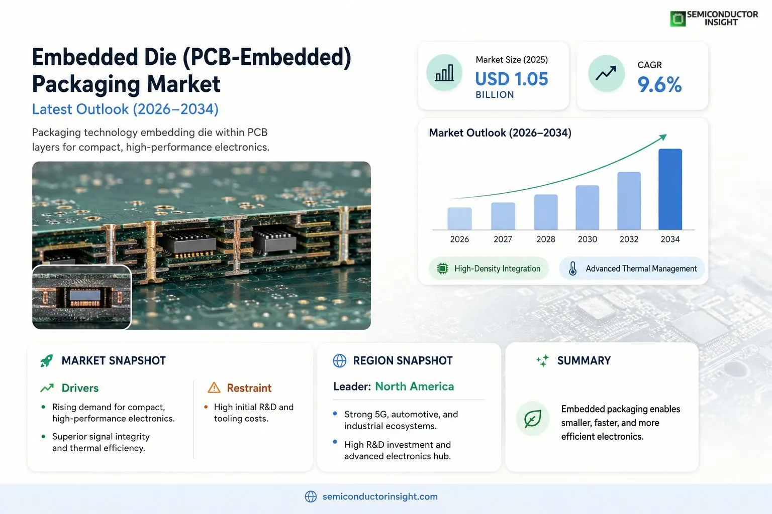
Global Embedded Die (PCB-Embedded) Packaging Market size was valued at USD 1.05 billion in 2025. The market is projected to grow from USD 1.18 billion in 2026 to USD 2.47 billion by 2034, exhibiting a CAGR of 9.6% during the forecast period.
Embedded Die (PCB-Embedded) Packaging refers to an advanced semiconductor packaging technology where bare semiconductor dies are embedded directly within the layers of a printed circuit board (PCB). This integration enhances electrical performance, reduces form factor, and improves thermal management, making it ideal for applications in high-density electronics such as smartphones, automotive electronics, IoT devices, and high-performance computing. The process involves embedding active or passive components into the substrate during PCB fabrication, enabling miniaturization while maintaining signal integrity and reliability.
The market is witnessing robust growth due to increasing demand for compact and high-performance electronic devices across industries. The rise of 5G technology, autonomous vehicles, and wearable electronics is accelerating adoption as manufacturers seek solutions that offer higher functionality in smaller footprints. Furthermore, advancements in materials science,such as improved dielectric substrates and conductive adhesives,are enhancing the feasibility and scalability of embedded die technologies. While challenges like high manufacturing complexity and design limitations persist, ongoing R&D investments by leading players such as AT&S, Schweizer Electronic AG, and TDK Corporation are driving innovation. For instance, in early 2024, AT&S announced a new production line dedicated to embedded component packaging for automotive radar modules, underscoring industry commitment to this transformative technology.
MARKET DRIVERS
Forced-Magnet Miniaturization
Embedded Die (PCB-Embedded) Packaging Market growth is significantly propelled by the rising consumer demand for smaller, lightweight electronics. As smartphones, wearables, and IoT devices continue to shrink, conventional through-hole and surface mount technologies reach their physical limits. Embedding passive components directly into the substrate offers a solution to these space constraints, allowing for more complex functionality in a smaller footprint. This drive towards highly compact electronic systems necessitates advanced packaging techniques that can integrate high-density components without compromising signal integrity.
Another critical driver is the demand for improved thermal management and electrical performance. By embedding die within the substrate, electrical path lengths are significantly reduced, which minimizes signal loss and EMI interference. This is particularly vital for high-frequency applications in consumer electronics and industrial automation. Furthermore, the ability to reduce noise and improve frequency response makes embedded packaging an attractive option for critical automotive and communication systems, accelerating the adoption of this technology across various industrial sectors.
➤ The integration of embedded die reduces the overall footprint of electronic assemblies by up to 40% in specialized high-density applications.
The continuous innovation in semiconductor and substrate manufacturing processes also acts as a major market catalyst. As manufacturers refine their ability to create robust substrates that can withstand reflow processes, the reliability of embedded components improves. This technological maturation lowers the barrier for adoption, allowing even smaller electronics companies to leverage the benefits of embedded die technology without requiring prohibitively expensive custom tooling or manufacturing setups.
MARKET CHALLENGES
Tech Complexity and Yield Rate
The transition to embedded packaging introduces significant complexity in the manufacturing process. Unlike standard assembly, embedding requires precise alignment and bonding of passive components to the inner layers of the board before the top cover layer is applied. This sequential process requires advanced machinery and rigorous quality control measures. Any slight variance in alignment or bonding pressure can result in interlayer stress, leading to defects that are difficult and expensive to detect post-assembly, thereby increasing the overall manufacturing complexity.
Other Challenges
Voice Coil Motor Assembly Reliability
In applications such as microphones and certain actuators, the integration of the die can impact the mechanical performance and reliability of the device. Ensuring the mechanical resonance of the embedded components remains optimal within the rigid board structure presents a unique engineering hurdle. Additionally, the difficulty in repairing or replacing embedded components once the board is sealed poses logistical challenges for repair facilities and end-of-life recycling processes.
Insufficient Standardization
Embedded Die (PCB-Embedded) Packaging Market currently lacks universally accepted standards for testing and qualification. Without industry-wide protocols, manufacturers face difficulties in validating their designs and ensuring interoperability between different component suppliers. This ambiguity can slow down the design cycle and increase development risks for OEMs relying on these specialized packaging techniques.
MARKET RESTRAINTS
High Initial R&D and Tooling Costs
One of the primary factors limiting the uptake of embedded die technology is the substantial upfront investment required for Research and Development and specialized tooling. Unlike traditional PCB assembly, embedded packaging demands high-precision drilling, lamination, and bonding equipment, all of which are expensive to procure and maintain. For smaller electronics manufacturers with limited capital allocation, the high entry barrier makes embedded packaging a less attractive option compared to proven, conventional assembly methods. This financial constraint is particularly restrictive in emerging economies where cost sensitivity is paramount.
Furthermore, the supply chain for specialized high-density substrates is less mature compared to standard FR4 materials. Manufacturers often face longer lead times and higher costs associated with sourcing the specific organic dielectric materials required for high-frequency embedded applications. This lack of supply chain maturity can lead to volatility in pricing and availability, creating further hesitation for large-scale industrial adoption of embedded die packaging.
MARKET OPPORTUNITIES
Automotive Electronics Application Expansion
The rapid proliferation of electric vehicles (EVs) and advanced driver-assistance systems (ADAS) presents a massive opportunity for Embedded Die (PCB-Embedded) Packaging Market. Modern vehicles contain thousands of passive components, and the need for space-saving, high-reliability electronics is critical. Embedded packaging can significantly reduce the weight and size of onboard ECU (Electronic Control Unit) systems, contributing to overall vehicle efficiency. As automotive manufacturers push for electric mobility and autonomous driving capabilities, the demand for robust, high-density embedded components is expected to surge.
Additionally, the growth of the Internet of Things (IoT) ecosystem opens new avenues for market expansion. The massive scale of IoT deployments requires ultra-compact sensors and nodes that can operate for years on low power. Embedded passive components offer the stability and miniaturization needed for these devices. By enabling developers to create smaller, more energy-efficient sensors, embedded packaging enables the further realization of smart cities and connected infrastructure projects.
Finally, advancements in Material Science related to High-Tg and halogen-free organic substrates are poised to unlock further potential. Developing substrate materials that can withstand higher processing temperatures and offer superior moisture resistance will enhance the reliability of embedded packages in harsh environments. This innovation will allow the technology to penetrate sensitive sectors such as aerospace and defense, where reliability under extreme conditions is non-negotiable.
Embedded Die (PCB-Embedded) Packaging Market Trends
Embedded Die (PCB-Embedded) Packaging is a crucial technology in modern electronics, directly integrating semiconductor dies into printed circuit boards. This approach is gaining traction as the demand for miniaturized and high-performance electronic devices surges across various sectors. The market is experiencing significant development, driven by the need for enhanced functionality within increasingly compact form factors.
Other Trends
Rising Demand in Automotive Electronics
The automotive industry is a key driver for Embedded Die (PCB-Embedded) Packaging Market. The proliferation of advanced driver-assistance systems (ADAS) and electric vehicle (EV) technologies necessitates high-reliability and compact electronic components. Embedded packaging enables the integration of various functionalities into smaller spaces, contributing to the development of more efficient and safer vehicles. Recent industry reports indicate a substantial increase in demand for these solutions specifically tailored for automotive radar and sensor modules.
Advancements in 5G Technology
The rollout of 5G networks has significantly boosted the demand for sophisticated electronic devices, including smartphones, base stations, and IoT infrastructure. Embedded Die (PCB-Embedded) Packaging plays a vital role in enabling the performance requirements of 5G devices by allowing for denser integration of components and improved signal integrity. The need for smaller, more power-efficient modules is directly fueling innovation in this packaging segment.
Growing Adoption in IoT Devices
The Internet of Things (IoT) market is expanding rapidly, with an increasing number of connected devices deployed across industries. Embedded Die (PCB-Embedded) Packaging is well-suited for IoT applications due to its ability to create compact, robust, and power-efficient modules. This technology allows for the integration of sensors, processors, and communication modules into small form factors, making it ideal for applications such as smart sensors, wearable devices, and industrial IoT equipment.
Focus on Thermal Management
As electronic devices become more powerful and densely packed, effective thermal management is becoming increasingly critical. Embedded Die (PCB-Embedded) Packaging offers inherent advantages in thermal dissipation, contributing to improved device reliability and performance. Innovative materials and design techniques are being implemented to enhance heat transfer capabilities within embedded packages, addressing the challenges posed by higher power densities.
COMPETITIVE LANDSCAPEKey Industry Players
Embedded Die (PCB-Embedded) Packaging Market
Embedded Die (PCB-Embedded) Packaging Market is characterized by a mix of established semiconductor packaging companies and specialized players focusing on advanced technologies. Key strategies employed by these companies include R&D investments in materials and processes, capacity expansions to meet growing demand, and strategic collaborations to broaden product portfolios and reach new markets. The market’s growth is significantly propelled by the increasing adoption of this technology in high-density electronic devices, particularly those within the automotive, IoT, and consumer electronics sectors. Companies are concentrating on enhancing the performance, reliability, and miniaturization aspects of embedded die packaging to cater to the evolving requirements of these industries.
Dominant players are actively engaged in developing innovative solutions to address the complexities of embedded die packaging, including challenges related to thermal management, signal integrity, and manufacturing yield. Several companies are expanding their offerings to include comprehensive packaging solutions, encompassing both embedded die and standard packaging technologies. Furthermore, partnerships between material suppliers, equipment manufacturers, and system integrators are becoming increasingly common to accelerate the adoption of this technology. The competitive landscape is dynamic, with ongoing innovation and mergers and acquisitions shaping the future of the market.
List of Key Embedded Die (PCB-Embedded) Packaging Companies Profiled
- AT&S
- AT&S</a/>
- Schweizer Electronic AG
- Schweizer Electronic AG
- TDK Corporation
- TDK Corporation
- Epcos (Murata Manufacturing Co., Ltd.)
- Amlogic
- Silvertree Semiconductor
- Vishay Intertechnology, Inc.
Segment Analysis:
| Segment Category | Sub-Segments | Key Insights |
| By Type |
|
Leading Segment exhibits strong adoption in high-performance computing due to its enhanced thermal management capabilities, enabling higher clock speeds and improved efficiency. |
| By Application |
|
Leading Segment in automotive electronics is driven by the increasing demand for advanced driver-assistance systems (ADAS) and autonomous driving capabilities, requiring compact and reliable electronic components. |
| By End User |
|
Leading Segment among consumer electronics manufacturers is witnessing increased adoption in premium devices requiring miniaturization and enhanced performance. |
| By Technology Node |
|
Leading Segment in advanced nodes is key for achieving the highest levels of integration and performance in cutting-edge electronic devices. |
| By Package Material |
|
Leading Segment utilizing ceramic substrates is prevalent in automotive applications due to their excellent thermal conductivity and reliability. |
Regional Analysis: North America
United States
Ongoing advancements in materials science and microfabrication are continuously improving the capabilities of Embedded Die (PCB-Embedded) Packaging. This includes the development of new thermal interface materials and advanced die attach techniques.
Embedded Die (PCB-Embedded) Packaging Market is experiencing a trend of consolidation, with larger players acquiring smaller, specialized companies to expand their product offerings and market reach.
Increasing environmental concerns are driving the adoption of more sustainable packaging solutions, including the use of eco-friendly materials and designs that minimize waste.
Geopolitical factors and recent disruptions have highlighted the importance of building resilient supply chains for Embedded Die (PCB-Embedded) Packaging components.
North America
The North American region, particularly the United States, is a dominant force in Embedded Die (PCB-Embedded) Packaging Market, boasting a robust ecosystem of technology providers, research institutions, and end-use industries. This region’s strong emphasis on innovation and its substantial investments in advanced electronics are key drivers of market growth. The demand for high-performance packaging is particularly pronounced in sectors such as aerospace and defense, telecommunications, and high-performance computing. The increasing complexity of electronic devices necessitates sophisticated packaging solutions for efficient heat dissipation, signal integrity, and miniaturization. Furthermore, the region’s established manufacturing infrastructure and skilled workforce provide a competitive advantage for companies operating in this space. The focus on next-generation technologies, including artificial intelligence and the Internet of Things, further reinforces North America’s position as a leading market for Embedded Die (PCB-Embedded) Packaging.
Europe
Europe presents a significant and steadily growing market for Embedded Die (PCB-Embedded) Packaging, with strong adoption in automotive, industrial automation, and medical device segments. The region’s focus on energy efficiency and sustainable technologies is driving demand for innovative packaging solutions that can optimize device performance and minimize energy consumption. Stringent regulatory standards regarding product safety and environmental impact also influence the types of packaging solutions adopted. The automotive industry, with its increasing reliance on advanced driver-assistance systems (ADAS) and electric vehicle technology, is a major consumer of Embedded Die (PCB-Embedded) Packaging. Furthermore, the growing industrial automation sector is driving demand for robust and reliable packaging solutions for embedded systems. Government initiatives supporting technological innovation and industrial competitiveness are also contributing to the growth of the market in Europe.
Asia-Pacific
The Asia-Pacific region is anticipated to be the fastest-growing market for Embedded Die (PCB-Embedded) Packaging, driven by rapid industrialization, increasing electronics production, and a burgeoning consumer market. Countries like China, Japan, and South Korea are key contributors to this growth, with substantial investments in semiconductor manufacturing and electronics assembly. The demand for high-performance packaging is particularly strong in the telecommunications and consumer electronics sectors. The rise of 5G and the Internet of Things are fueling the need for advanced packaging solutions that can support high data transfer rates and low power consumption. Furthermore, the region’s cost-competitive manufacturing environment is attracting investment from global packaging companies. Government support for the electronics industry is also playing a crucial role in driving market expansion.
South America
South America represents a relatively smaller but promising market for Embedded Die (PCB-Embedded) Packaging, with growth opportunities in the industrial, telecommunications, and automotive sectors. The increasing adoption of electronics in various industries and the growing demand for connected devices are key drivers of market expansion. The region’s expanding industrial base, particularly in Brazil and Argentina, is driving demand for packaging solutions for industrial automation and control systems. The telecommunications sector is also witnessing growth, fueled by the rollout of 4G and 5G networks. Furthermore, the automotive industry is experiencing increasing demand for sophisticated electronics and embedded systems, creating opportunities for specialized packaging solutions. However, economic uncertainties and infrastructure limitations pose challenges to market growth in the region.
Middle East & Africa
The Middle East and Africa region presents a nascent but potentially high-growth market for Embedded Die (PCB-Embedded) Packaging, driven by increasing investments in infrastructure development, telecommunications, and renewable energy. The growth of the telecommunications sector, particularly the deployment of 5G networks, is a major driver of demand for advanced packaging solutions. The increasing adoption of smart city initiatives and the development of industrial sectors are also contributing to market expansion. Furthermore, the region’s growing automotive industry is creating demand for packaging solutions for connected vehicles and electric vehicles. However, political instability and economic challenges in some countries pose obstacles to market growth.
Report Scope
This market research report provides a comprehensive analysis of the Embedded Die (PCB-Embedded) Packaging Market , covering the forecast period 2026–2034. It offers detailed insights into market dynamics, technological advancements, competitive landscape, and key trends shaping the industry.
Key focus areas of the report include:
- Market Overview: The report begins with an overview outlining its current market scenario, key growth indicators, and industry transformation drivers. It discusses macroeconomic factors, demand–supply balance, regulatory landscape, and the strategic role of semiconductors in powering advancements across industries such as automotive, telecommunications, consumer electronics, and industrial automation.
- Market Size & Forecast: Historical data and future projections for revenue, unit shipments, and market value across major regions and segments.
- Segmentation Analysis: Detailed breakdown by product type, technology, application, and end-user industry to identify high-growth segments and investment opportunities.
- Regional Insights: Insights into market performance across North America, Europe, Asia-Pacific, Latin America, and the Middle East & Africa, including country-level analysis where relevant.
- Competitive Landscape: Profiles of leading market participants, including their product offerings, R&D focus, manufacturing capacity, pricing strategies, and recent developments such as mergers, acquisitions, and partnerships.
- Technology Trends & Innovation: Assessment of emerging technologies, integration of AI/IoT, semiconductor design trends, fabrication techniques, and evolving industry standards.
- Market Drivers & Restraints: Evaluation of factors driving market growth along with challenges, supply chain constraints, regulatory issues, and market-entry barriers.
- Stakeholder Insights: Insights for component suppliers, OEMs, system integrators, investors, and policymakers regarding the evolving ecosystem and strategic opportunities.
Primary and secondary research methods are employed, including interviews with industry experts, data from verified sources, and real-time market intelligence to ensure the accuracy and reliability of the insights presented.
FREQUENTLY ASKED QUESTIONS:
What is the current market size of Embedded Die (PCB-Embedded) Packaging Market?
-> Embedded Die (PCB-Embedded) Packaging Market was valued at USD 1.05 billion in 2025 and is expected to reach USD 2.47 billion by 2034, reflecting a CAGR of 9.6% over the forecast period.
Which key companies operate in Embedded Die (PCB-Embedded) Packaging Market?
-> Key players include AT&S, Schweizer Electronic AG, and TDK Corporation, among others.
What are the key growth drivers?
-> Key growth drivers include the rollout of 5G technology, the emergence of autonomous vehicles, and the rise of wearable electronics demanding compact, high‑performance packaging solutions.
Which region dominates the market?
-> The reference does not specify a dominant region.
What are the emerging trends?
-> Emerging trends include advancements in dielectric substrate materials, the use of conductive adhesives for improved scalability, and dedicated production lines for automotive radar modules.

Get Sample Report PDF for Exclusive Insights
Report Sample Includes
- Table of Contents
- List of Tables & Figures
- Charts, Research Methodology, and more...
 Download Sample Report PDF