Key Statistics
Key Takeaways
- Back-end revenue: Display driver chip packaging and testing generated an estimated USD 3,622.6 million in 2025 and is projected to reach USD 6,548.8 million in 2034. Demand follows panel-device designs, testing complexity and outsourced finishing of driver integrated circuits rather than the full value of finished screens.
- Packaging dominance: Chip Packaging captures an estimated ~68% of activity; gold bumping, wafer thinning, chip-on-film inner-lead bonding and shipment-ready die preparation require multiple production steps. Chip Testing contributes an estimated ~32%, with probe quality and electrical screening especially important for high-pin-count drivers.
- End-use concentration: Consumer Electronics represents an estimated ~58% of 2025 revenue as television and handset display ICs require high-volume assembly and repeatable screening. Vehicle Electronics accounts for an estimated ~18%, benefiting from wide dashboards and stringent thermal-cycle demands. Across the 2026–2034 forecast, the headline 6.8% CAGR reflects gradual product upgrading rather than a uniform increase in every panel type.
- Geographic concentration: Asia-Pacific holds an estimated ~67% share, reflecting Taiwan-based display driver OSAT capacity, Chinese panel production and Korean device customers. North America accounts for an estimated ~18% largely through end-device demand, IP ownership and engineering relationships rather than comparable driver-assembly capacity.
- Margin constraints: Packaging suppliers face aggressive panel-maker pricing and expensive equipment qualification; a 2025 ChipMOS filing described a fall in display driver assembly and testing revenue under weak panel demand. Fine-pitch OLED transitions nevertheless reward well-controlled bump metallurgy and film bonding.
Display Driver Chip Packaging and Testing Market Overview
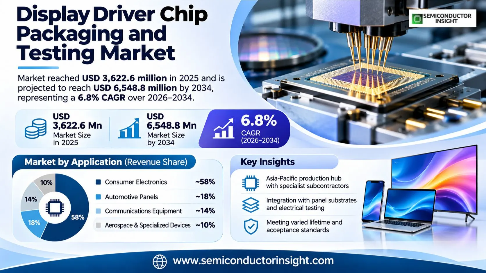
Display driver chip packaging and testing market reached USD 3,622.6 million in 2025 and is projected to reach USD 6,548.8 million by 2034, representing a 6.8% CAGR over 2026–2034. Production is concentrated in Asia-Pacific, where specialist subcontractors connect driver dies to panel substrates and electrically screen them before module assembly.
Display driver integrated circuits sit between image-processing electronics and the individual pixels in LCD and OLED panels. Packaging converts semiconductor wafers into dies that can connect to glass or flexible-film electrodes, while testing checks output channels, leakage, timing and power behavior before display makers commit the part to a panel. Commercial contracts are often split across wafer bumping, probing, tape assembly and final electrical tests, giving specialized OSAT businesses several points of participation.
The revenue boundary covers contracted back-end processing and testing specifically undertaken for display driver chips. It includes chip-on-glass die preparation, chip-on-film bonding, bump metallurgy, related die handling and electrical verification. It excludes the value of finished televisions, smartphones, display modules, semiconductor design licenses and fabrication of the original silicon wafer unless a service is part of the described driver finishing process.
Panel architecture alters the package cost structure. Flexible OLED smartphones favor narrow bezels and fine electrode pitches, requiring very small bumps and careful control of bending stress where flexible substrate meets rigid silicon. Larger televisions often use chip-on-film connections to reach fine traces across broad panel edges, whereas automotive panels add a premium for long qualification cycles and resistance to cockpit temperature swings.
Supplier economics depend on throughput as much as selling price. Poor probe yield can trigger expensive rework after high-value gold deposition, and film-tape misalignment can make a fully functional driver unusable. Foundry and display manufacturer schedules are therefore matched to equipment uptime, materials traceability and qualified assembly recipes. Capital is committed before the factory can recover investment across multiple driver variants.
Segment Analysis: By Type
Chip Packaging represents an estimated ~68% of display-driver back-end service revenue in 2025. This includes thinning and singulation, bump formation and physical assembly in formats such as chip-on-glass and chip-on-film. Chip Testing contributes an estimated ~32% through probing and end-of-line characterization; the growing number of outputs in advanced panels makes electrical coverage an important commercial differentiator.
| Type | Function | Market position |
|---|---|---|
| Chip Packaging | Estimated ~68% of 2025 sales. Driver wafers receive metal bumps with tightly controlled height before being singulated into individual chips. Some dies ship for direct glass-panel assembly; others are thermocompression-bonded to flexible film that routes signals toward panel electrodes. Process control must minimize wafer cracking, bump voids and damage to narrow leads. Packaging houses compete on high-volume yield, film availability and the speed with which new panel generations qualify. | |
| Chip Testing | Estimated ~32% of 2025 sales. Wafer-level probe cards and final functional testers verify display outputs, signal timing, current consumption and defective channels. A driver can meet basic logic specifications yet still create visible line defects when bonded to a screen; test plans therefore target faults that become costly after panel assembly. Higher-resolution displays require effective pin-contact maintenance, test parallelism and clear failure-bin traceability across customer lots. |
Segment Analysis: By Application
Consumer Electronics accounts for an estimated ~58% of outsourced display-driver packaging and test activity, supported by smartphones, notebooks, televisions and wearable displays. Automotive panels provide the next-largest application at an estimated ~18%. Communications equipment, aerospace instrumentation and specialized devices form smaller but technically distinctive groups whose product lifetimes and acceptance standards can justify different commercial terms.
| Application | Demand characteristics |
|---|---|
| Consumer Electronics | Estimated ~58% share. Handsets and televisions create the largest recurring lot sizes, but their seasonal ordering can expose subcontractors to utilization swings. OLED phone panels value narrow-bezel chip-on-plastic and chip-on-film attachment, while LCD television driver packages must support long channel runs and low per-panel cost. High volume puts pressure on contract prices, making scrap reduction and tester efficiency decisive for factory profitability. |
| Vehicle Electronics | Estimated ~18% share. Digital instrument clusters, passenger displays and central infotainment panels require driver connections resilient to vibration and automotive thermal cycling. Vehicle programs typically maintain a chosen display architecture over longer periods than phone models, giving certified subcontractors more predictable production after qualification. Screening must identify latent interconnect problems before a failure becomes a visible cabin defect or service claim. |
| Communication | Estimated ~12% share. Video conferencing terminals, monitoring consoles and networking equipment use LCD or OLED displays for operator interaction. Packaging demand in these products follows comparatively specialized module orders rather than consumer handset volumes. Customer acceptance often emphasizes stable color output, connector reliability and the ability to reproduce a qualified film-bond recipe when equipment makers refresh their device platforms. |
| Aerospace | Estimated ~4% share. Cockpit, ground-control and specialist information displays can demand extended traceability and stringent environmental verification. The driver package itself is only one component in an approved display chain, so suppliers may face long review cycles and modest annual quantities. The attraction is more demanding engineering work and potentially durable procurement relationships, not mass-volume fabrication of commercial aircraft systems. |
| Other | Estimated ~8% share. Industrial operator panels, medical instrumentation and unusual form-factor devices require driver circuits packaged for specific substrate dimensions and service conditions. Some customers prioritize lifecycle continuity over aggressive reduction in assembly price. Smaller production runs can increase setup charges, so engineering documentation, sample turnaround and a practical route to repeat testing influence whether a subcontractor wins the order. |
Regional Analysis
Display-driver back-end operations cluster near semiconductor, film-tape and display-panel manufacturers. Asia-Pacific accounts for an estimated ~67% of 2025 value, followed by North America ~18%, Europe ~10%, South America ~3% and Middle East & Africa ~2%. These estimates concern the packaging and testing service market, not overall sales of screens or finished electronics.
Where is display driver chip packaging and testing capacity most concentrated?
The strongest customer-supplier links connect Taiwan-based driver IC test and bump specialists with panel makers and IC designers throughout East Asia. North American and European demand is more heavily associated with electronics design, automotive displays and specialized qualification. Production footprints can cross borders within a single order: a wafer may be fabricated in one jurisdiction, bumped and screened in another, and finally attached to a display module elsewhere.
| Region | Position | Growth outlook | Demand profile | What decides supplier selection |
|---|---|---|---|---|
| Asia-Pacific | An estimated ~67% | ~7.5% CAGR | Taiwan specialist OSATs with China, Korea and Japan panel ecosystems | Fine-pitch COF and OLED display assembly underpin service demand |
| North America | An estimated ~18% | ~6.2% CAGR | United States semiconductor design and automotive display integration | High-reliability qualification and design relationships support contracts |
| Europe | An estimated ~10% | ~5.8% CAGR | German automotive cockpit engineering and display-module suppliers | Long vehicle qualification cycles shape outsourced assembly orders |
| South America | An estimated ~3% | ~5.1% CAGR | Brazilian equipment and electronics assembly with limited local OSAT depth | Imports and module integration dominate purchasing economics |
| Middle East & Africa | An estimated ~2% | ~4.8% CAGR | Israeli IC engineering and Gulf electronics infrastructure | Specialized integration and imported finished driver units prevail |
Key Display Driver Chip Packaging and Testing Manufacturers and Competitive Landscape
The competitive landscape includes Chipbond Technology, ChipMOS Technologies, Steco, LB-Lusem, JCET, Tongfu Microelectronics and specialist Asian display-driver subcontractors. Their offerings differ by gold-bump capability, tape-bond equipment, wafer-probe know-how and the degree of integration from incoming wafers to final-tested driver assemblies. Client approval operates at the level of particular lead pitches and materials, so a large multi-category OSAT cannot simply transfer all of its equipment to a driver job. Repeatable test vectors and customer response speed help suppliers retain recurring contracts when panel makers redesign an attachment format.
Chipbond describes wafer bumping, chip-on-glass, chip-on-film and chip-on-plastic technologies as distinct services, giving customers several routes to reach the panel electrode geometry they need. A process breadth advantage is most valuable when a display designer expects multiple package variants. However, qualification remains recipe-specific: a supplier that builds LCD COG parts cannot automatically substitute its line for an OLED flexible-panel job without additional validation.
ChipMOS offers wafer test, bumping, assembly and final test, and its 2025 regulatory filing separately reported display panel driver assembly and testing revenue. The company attributed a year-on-year decrease in that revenue group to weaker customer demand, inventory adjustment and pricing pressure in mainland China. This illustrates the importance of balancing specialist driver capacity against volatile orders rather than equating facility capability with a fixed revenue stream.
Tier structure
| Tier | Companies | Basis of competition |
|---|---|---|
| Integrated display-driver OSAT specialists | Chipbond Technology; ChipMOS Technologies; Steco; LB-Lusem | Specialists control bump geometry, tape bonding and associated electrical checks. Their advantage is detailed manufacturing knowledge accumulated through multiple generations of LCD and OLED driver designs, together with factory procedures that support high throughput and rapid troubleshooting. |
| Diversified packaging and testing groups | JCET Group; Tongfu Microelectronics; ASE Technology Holding; Hefei Chipmore | Broader contract assembly providers can offer alternative backend capacity and relationships with IC designers. A diversified supplier may support several component classes, but actual eligibility for a driver program depends on fine-pitch tooling, customer approval and appropriate module interconnect know-how. |
Key companies profiled
- Chipbond Technology
- ChipMOS Technologies
- Steco
- LB-Lusem
- JCET Group
- Tongfu Microelectronics
- ASE Technology Holding
- Hefei Chipmore
Display Driver Chip Packaging and Testing Production Capacity Analysis
Useful production capacity is determined by qualified bump plating, probe throughput, high-speed film bonding and dependable device sorting rather than building area alone. Flexible OLED packages can require more sophisticated interconnect control than conventional LCD display drivers, so nominal wafer throughput may overstate immediately available capacity for a particular fine-pitch customer program. ChipMOS has listed 14 micrometer inner-lead pitch in its 2026 development roadmap, indicating the degree of precision sought for future fine-pitch COF production.
(‘Bump and bond bottlenecks’, ‘Gold deposition uniformity and precision lithography influence whether a driver wafer can be assembled with a sufficiently small pitch. Chip-on-film production additionally requires high-speed thermocompression, correctly prepared flexible tape and stable adhesive curing. Yield losses at any stage can erase the efficiency gained from faster bonding equipment. Capacity planning therefore considers complete qualified process routes, not isolated machine counts.’)
(‘Testing economics and utilization’, ‘Wafer probe and final electrical test programs must check large numbers of display outputs while retaining acceptable cycle time. Parallel test heads can improve throughput, but contactor maintenance, equipment calibration and engineering change control become more demanding. When panel orders weaken, specialized tester and bonding utilization can fall before labor or equipment expenses adjust, increasing the unit cost of processed display drivers.’)
Display Driver Chip Packaging and Testing Market Dynamics: Drivers, Restraints and Opportunities
Smartphone OLED adoption, large-screen viewing preferences and increasingly sophisticated vehicle dashboards raise the need for reliable driver interconnects. Growth is offset by price negotiations, material cost pressure and substantial development expense when a production partner must shift to fine-pitch panel technology. The two impact tables show the relative influence of these forces on the forecast trajectory.
MARKET DRIVERS
Drivers Impact Analysis*
| Market Drivers | Impact Rank | CAGR Contribution (%) | 2026–2028 | 2029–2031 | 2032–2034 |
|---|---|---|---|---|---|
| Consumer OLED and high-resolution panel orders | High | +4.20% | High | High | High |
| Vehicle cockpit and infotainment display expansion | Medium-High | +2.50% | Medium | High | High |
| Fine-pitch COF and flexible display innovation | Medium | +1.50% | Medium | High | High |
| Longer-life industrial and medical screen platforms | Low-Medium | +0.90% | Medium | Medium | Medium |
| Others (wearables and communications displays) | Low | +0.40% | Low | Medium | Medium |
Consumer OLED migration
Flexible OLED panels require compact package formats and a high-quality connection between rigid silicon and bendable film. Suppliers that can maintain bump height, lead alignment and adhesive integrity benefit when device makers pursue slimmer borders. The commercial payoff is tied to qualified shipments and repeat orders: engineering samples alone do not deliver the utilization required to amortize new packaging equipment.
Automotive multi-screen adoption
Modern cockpits can contain separate driver packages for clusters, passenger screens and central controls. Automotive customers require extended reliability data and expect controlled component modifications over multiple years. Packaging vendors therefore earn opportunities to supply higher-value validated processes, although initial qualification and service documentation may absorb more engineering resources than comparable consumer lots.
Advanced bonding geometries
New chip-on-plastic structures and ultra-fine-pitch chip-on-film interconnects can increase the technical content of each driver assembly contract. The challenge involves low-damage wafer handling, plated-pad accuracy and reliable electrical contact to increasingly dense traces. Contract factories that integrate those capabilities reduce handoffs and can support panel makers as display designs change without abandoning proven driver functionality.
MARKET RESTRAINTS
Restraints Impact Analysis*
| Market Restraints | Impact Rank | CAGR Contribution (%) | 2026–2028 | 2029–2031 | 2032–2034 |
|---|---|---|---|---|---|
| High capital investment and qualification charges | High | -1.30% | High | Medium | Medium |
| Panel-cycle pricing pressure and inventory corrections | Medium | -0.80% | High | Medium | Low |
| Others (tape, bump materials and cross-border logistics) | Low | -0.60% | Medium | Medium | Low |
Investment and process qualification
Electroplating, precision lithography, advanced probe cards and film-bonding equipment are expensive to install and maintain. A customer may demand a dedicated test program and a lengthy series of reliability lots before releasing volume. This delays cash recovery and can make smaller driver-design programs unattractive to subcontractors without flexible multi-customer tool scheduling.
Aggressive display supply-chain pricing
Panel makers and driver designers frequently revise pricing when screen inventory grows or consumer demand weakens. Specialized service providers face the same fixed equipment charges despite lower lot volumes. ChipMOS reported a decline in its 2025 display panel driver assembly and test business, demonstrating how market softness and competition can flow directly into OSAT results.
Materials and logistics exposure
Gold bump materials, qualified flexible tapes and special adhesives may have long ordering lead times or limited approved suppliers. Substituting a chemical or film can change bond performance and require fresh customer trials. Cross-border wafer movement also complicates forecasting, because packaging lines need matching incoming wafers, known design revisions and the correct finished-panel destination to operate efficiently.
MARKET OPPORTUNITIES
Foldable phone driver technology
Foldable OLED modules place flexible interconnects under repeated mechanical stress and tight dimensional limits. A process house capable of controlled chip-on-plastic packaging and consistent protective films can participate in premium product designs. Engineers must demonstrate stability across bending and heat exposure, so differentiated service value comes from documented reliability rather than merely offering the newest interconnect label.
Automotive display validation
Long-running vehicle programs create incentives to maintain approved driver assembly recipes over several years. Suppliers can combine early engineering support with documented production screening and planned replacement materials. Automotive contracts are not guaranteed volume, but successful qualification can reduce competitive turnover when changing a package would trigger broader display-module revalidation.
Process integration for panel designers
Display IC manufacturers increasingly need a coordinated path from incoming wafers through bump deposition and final electrical acceptance. A factory with aligned probe, bonding and defect-analysis teams can shorten feedback cycles when a customer changes electrode pitch. Better root-cause isolation improves the chance that new driver products reach volume without costly repeated pilot lots.
Display Driver Chip Packaging and Testing Supply Chain Analysis
The display driver back-end chain begins with fabricated driver wafers and continues through metallization, electrical wafer sort, singulation, flexible-film or glass attachment and final tests. Multiple specialists may take part, but each must retain lot records so a panel maker can trace visual defects to the correct processing stage. Wafer test records and film-bond results must remain linked across factory transfers. Where panels show visible pixel-line failure after module integration, this history helps determine whether the cause is intrinsic silicon, poor metallization or an unsuitable connection to the flexible substrate.
Wafers and design revisions. The incoming semiconductor wafer carries a dense pattern of display-output pads whose geometry must match the planned packaging process. A small change to pad pitch can make a previously approved bump mask or bond recipe unsuitable. Subcontractors therefore establish configuration controls before processing high-value lots. Matching design files to wafer identity also helps failure-analysis teams attribute an open circuit to the correct manufacturing step.
Qualified metallization materials. Gold and alternative Cu/Ni/Au bump structures provide the electrical interface between the driver and the module substrate. Material choice affects pitch, corrosion resistance and thermocompression behavior. Purchase decisions involve approved electroplating chemistry and process repeatability, not just commodity metal prices. Chemical changes are treated cautiously because they can alter long-term contact reliability even when initial resistance measurements appear acceptable.
Flexible substrates and adhesives. Chip-on-film lines rely on flexible circuit tapes and protective compounds whose thermal expansion and moisture response influence bond strength. Some large-panel designs need additional stiffeners or heat-spreading attachments. Because a weak inner-lead bond can break under handling, manufacturers use controlled curing and mechanical checks. A service provider with qualified tape suppliers can often resolve assembly defects faster than one dependent on a single untested material option.
Fault traceability after delivery. The finished display chip often travels to a separate panel-module factory, where an image defect may appear during the final screen test. Package and test records help distinguish wafer electrical faults from bond misalignment or panel-electrode damage. Clear responsibility boundaries reduce wasteful returns and support early corrective action. Shipment scheduling must accommodate this feedback cycle when a display customer ramps a new high-resolution product line.
Recent Developments in the Display Driver Chip Packaging and Testing Market
- 20 January 2026 NOVATEK CARBON-FOOTPRINT VERIFICATION
Novatek said it had completed verification of the carbon footprint for its LCD driver IC products in 2024 and for the first phase of SoC devices in 2025. The company described product manufacturing, packaging and testing as components of its lifecycle analysis. For outsourced backend suppliers, this strengthens the commercial relevance of documented material inputs and processing energy, although the announcement is not a measure of packaging service market revenue. Source - 26 February 2026 NOVATEK DESIGN IP CONTROLS
Novatek announced that it retained an A-level certification under Taiwan’s intellectual-property management system for 2025. Its identified product portfolio includes display driver integrated circuits and smart imaging solutions. The event highlights the importance of protecting customer design information when wafers and test parameters pass between chip designers and packaging subcontractors; it should not be interpreted as additional assembly capacity. Source - 2026 annual-report cycle CHIPMOS ULTRA-FINE-PITCH COF ROADMAP
ChipMOS listed development of 14-micrometer inner-lead pitch COF flip-chip packaging among its 2026 research plans, alongside low-temperature materials for redistribution layers. Such work addresses the narrow interconnect spacing of advanced display devices, where tape alignment and contact metallurgy can become limiting yield factors. A stated development plan is distinct from a confirmed high-volume commercial launch. Source - July 2026 SEMI BACK-END EQUIPMENT FORECAST
SEMI forecast global assembly and packaging equipment sales of USD 6.7 billion in 2026 and semiconductor test equipment sales of USD 15.3 billion. These are equipment categories across all semiconductor types, not display driver services alone. The announcement nevertheless supplies context on investments in testing and packaging process capability as subcontractors decide which product families deserve additional capital. Source - 2 November 2026 INDIA BACK-END TESTING CAPACITY DISCUSSION
EE Times India examined the challenge of building semiconductor test capability as Indian OSAT operations expand, citing equipment demand and engineering constraints. The account reflects adjacent capacity conditions rather than a display driver assembly announcement. It nevertheless illustrates why test program flexibility, operator knowledge and stable throughput are central when a new manufacturing region seeks to support specialized device families. Source
REPORT SCOPE & SEGMENTATION
| Attribute | Details |
|---|---|
| Study Period | 2020–2034 |
| Base Year | 2025 |
| Estimated Year | 2026 |
| Forecast Period | 2026–2034 |
| Historical Period | 2020–2024 |
| Market Size Unit | USD million |
| 2025 Market Value | USD 3,622.6 million |
| 2034 Market Forecast | USD 6,548.8 million |
| Growth Rate | 6.8% |
| Largest Regional Market | Asia-Pacific |
| Market Coverage | Global display driver chip packaging and testing services |
| By Type | Chip Packaging; Chip Testing |
| By Application | Communication; Consumer Electronics; Vehicle Electronics; Aerospace; Other |
| By Region | Five regional markets evaluated across packaging capability, downstream panel demand and supplier qualification. Asia-PacificTaiwan, China, South Korea North AmericaUnited States, Canada, Mexico EuropeGermany, France, United Kingdom South AmericaBrazil, Argentina, Chile Middle East & AfricaIsrael, United Arab Emirates, South Africa |
| Key Companies Profiled | Chipbond Technology; ChipMOS Technologies; Steco; LB-Lusem; JCET Group; Tongfu Microelectronics; ASE Technology Holding; Hefei Chipmore |
| Customization Scope | Additional analysis can examine OLED fine-pitch bonding, customer reliability requirements, wafer-probe test costs and emerging flexible display assembly services. |
Frequently Asked Questions
What is the 2025 market size and 2034 outlook?
Display driver chip finishing and verification is estimated at USD 3,622.6 million in 2025 and is expected to reach USD 6,548.8 million in 2034, equivalent to 6.8% annualized growth. These values describe packaging and testing services associated with display driver semiconductors; they do not represent gross display-panel sales or revenue from finished devices.
Which processing activity accounts for most value?
Chip Packaging accounts for an estimated ~68% of activity because it combines bump plating, wafer thinning and either direct glass or flexible-film attachment, all requiring dedicated equipment and controlled handling. Chip Testing represents an estimated ~32%, but its contribution to defect detection can be disproportionately important when an undetected bad driver would compromise an expensive display module.
Which customer application is largest?
Consumer Electronics is the largest application at an estimated ~58% of 2025 demand, reflecting smartphone, television, computer and wearable display orders. The sourcing environment is highly cyclical. A large customer may request rapid capacity changes during product launches, then cut orders when panel inventories rise, challenging the utilization of specialized bump and bonding lines.
Where is back-end display driver manufacturing most concentrated?
Asia-Pacific accounts for an estimated ~67% of market activity. Taiwan provides established display-driver OSAT operations, China is a major downstream panel-making center, and South Korea supplies high-end OLED demand. These countries occupy different positions in the chain; one unit can cross borders several times before it becomes part of a working display.
What is the difference between COG and COF?
Chip-on-glass attaches the integrated circuit to glass-panel connections, while chip-on-film first connects it to flexible conductive tape. COF offers routing flexibility and can support thin panel borders, but introduces challenges involving film movement and inner-lead bond protection. The customer chooses the attachment approach based on display geometry, reliability requirements and approved manufacturing processes.
How are flexible OLED displays changing packaging requirements?
Flexible OLED designs seek narrow bezels and dense electrical connections. Chip-on-plastic and fine-pitch tape bonding help fit a driver circuit into a constrained mechanical area, though those features can increase alignment difficulty. Manufacturers must verify that plated contacts and protective materials withstand repeated assembly stress without intermittent pixel-line failures appearing in finished screens.
Why does electrical testing matter after wafer processing?
A chip can have correct internal logic yet a defective output channel that becomes visible only after panel connection. Wafer probing and final testing check performance limits and screen-relevant fault modes before a device is installed in a high-value module. Strong test coverage reduces the cost of downstream rejects, although extra screening time must be balanced against factory throughput.
Who are the principal packaging and testing suppliers?
Chipbond and ChipMOS are established display-driver service specialists, and the competitive field also includes Steco, LB-Lusem and larger packaging groups such as JCET and Tongfu. Capabilities differ across wafer bumping, fine-pitch tape assembly, probe technology and final test. Buyers must verify the exact qualified package format rather than treating every OSAT factory as a substitute.
What restricts service-provider profitability?
Specialist plating, bonding and test assets require heavy investment and ongoing calibration while display demand moves with consumer device cycles. Pricing pressure can be especially sharp during panel inventory corrections. Material substitutions may also require customer qualification, limiting how quickly a factory can respond to input cost changes and making high yield essential to sustained margins.
What should buyers verify before selecting a subcontractor?
Procurement teams should ask for package-specific process capability, bump-height controls, test coverage, failure-analysis support and lot traceability. A supplier should also demonstrate qualified flexible-film and adhesive inputs, stable equipment maintenance and a clear schedule for engineering changes. Confirmed display-driver capacity is more informative than company-wide semiconductor packaging revenue or an announcement about future technology development.
Research Sources & Evidence Base

Get Sample Report PDF for Exclusive Insights
Report Sample Includes
- Table of Contents
- List of Tables & Figures
- Charts, Research Methodology, and more...
 Download Sample Report PDF