Cutting-Edge Processes Wafer Foundry Market Overview
Cutting-edge wafer foundries are crucial for manufacturing advanced semiconductor chips, supporting industries such as high-performance computing (HPC), artificial intelligence (AI), and next-generation consumer electronics. Currently, TSMC, Samsung Foundry, and Intel Foundry Services (IFS) are the primary players providing advanced process nodes like 2nm, 3nm, 4nm, 5nm, and 7nm. The rising demand for AI, IoT, and HPC applications is driving the expansion of this market.
This report provides a deep insight into the global Cutting-Edge Processes Wafer Foundry market covering all its essential aspects. This ranges from a macro overview of the market to micro details of the market size, competitive landscape, development trend, niche market, key market drivers and challenges, SWOT analysis, value chain analysis, etc.
The analysis helps the reader to shape the competition within the industries and strategies for the competitive environment to enhance the potential profit. Furthermore, it provides a simple framework for evaluating and accessing the position of the business organization. The report structure also focuses on the competitive landscape of the Global Cutting-Edge Processes Wafer Foundry Market, this report introduces in detail the market share, market performance, product situation, operation situation, etc. of the main players, which helps the readers in the industry to identify the main competitors and deeply understand the competition pattern of the market.
In a word, this report is a must-read for industry players, investors, researchers, consultants, business strategists, and all those who have any kind of stake or are planning to foray into the Cutting-Edge Processes Wafer Foundry market in any manner.
Cutting-Edge Processes Wafer Foundry Market Analysis:
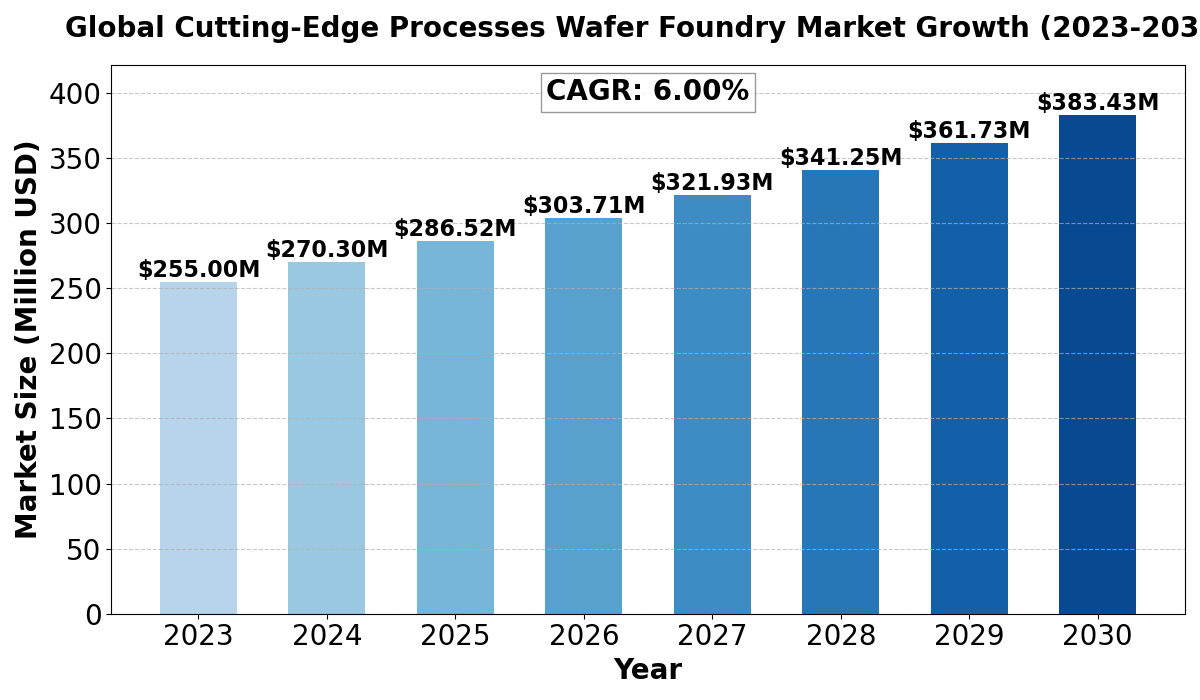
The global Cutting-Edge Processes Wafer Foundry market size was estimated at USD 255 million in 2023 and is projected to reach USD 383.43 million by 2030, exhibiting a CAGR of 6.00% during the forecast period.
North America Cutting-Edge Processes Wafer Foundry market size was USD 66.45 million in 2023, at a CAGR of 5.14% during the forecast period of 2025 through 2030.
Cutting-Edge Processes Wafer Foundry Key Market Trends :
- Transition to 2nm Process Nodes – The semiconductor industry is advancing toward 2nm technology, improving transistor density and power efficiency for AI, HPC, and mobile applications.
- Rising Demand for AI and HPC Chips – AI and high-performance computing applications require more efficient and powerful chips, fueling the growth of advanced wafer foundries.
- Expanding Foundry Capacities – Key players are making significant investments in expanding semiconductor fabrication facilities to meet growing demand and enhance production capabilities.
- Government Initiatives for Semiconductor Independence – Nations worldwide are increasing investments in semiconductor manufacturing to reduce reliance on foreign foundries and strengthen domestic production.
- Breakthroughs in EUV Lithography – Extreme Ultraviolet (EUV) lithography is enabling the production of smaller, more efficient chips, accelerating advancements in wafer foundry technologies.
Cutting-Edge Processes Wafer Foundry Market Regional Analysis :

- North America:Strong demand driven by EVs, 5G infrastructure, and renewable energy, with the U.S. leading the market.
- Europe:Growth fueled by automotive electrification, renewable energy, and strong regulatory support, with Germany as a key player.
- Asia-Pacific:Dominates the market due to large-scale manufacturing in China and Japan, with growing demand from EVs, 5G, and semiconductors.
- South America:Emerging market, driven by renewable energy and EV adoption, with Brazil leading growth.
- Middle East & Africa:Gradual growth, mainly due to investments in renewable energy and EV infrastructure, with Saudi Arabia and UAE as key contributors.
Cutting-Edge Processes Wafer Foundry Market Segmentation
The research report includes specific segments by region (country), manufacturers, Type, and Application. Market segmentation creates subsets of a market based on product type, end-user or application, Geographic, and other factors. By understanding the market segments, the decision-maker can leverage this targeting in the product, sales, and marketing strategies. Market segments can power your product development cycles by informing how you create product offerings for different segments.
Key Company
- HORIBA STEC
- Brooks Instrument
- Annealsys
- Kemstream
- TSI Incorporated (MSP)
- Lintec
- Fujikin Incorporated
- Bronkhorst
- RASIRC
- Air Liquide
- SEMPA
Market Segmentation (by Type)
- DLI-CVD
- DLI-ALD
- Others
Market Segmentation (by Application)
- Semiconductor Production Processes
- Research & Development, and Pilot
Drivers
- Increasing Demand for AI and 5G Technologies – AI, 5G, and IoT applications require high-performance chips, driving demand for cutting-edge wafer foundries.
- Advancements in Semiconductor Manufacturing – Technologies like EUV lithography and FinFET transistors are enhancing chip efficiency, contributing to market growth.
- Rising Investments in Chip Fabrication – Key foundry players are expanding production capacities to address the growing need for advanced semiconductor chips.
Restraints
- High Manufacturing Costs – The cost of setting up and maintaining cutting-edge wafer foundries is extremely high, limiting new market entrants.
- Supply Chain Constraints – The semiconductor industry faces ongoing challenges related to raw material shortages and geopolitical trade restrictions.
- Limited Number of Market Players – Only a few companies have the expertise and resources to develop 2nm and 3nm technologies, restricting competition.
Opportunities
- Growth in Edge Computing and IoT Devices – The increasing adoption of IoT and edge computing devices presents new opportunities for advanced wafer foundries.
- Strategic Partnerships and Collaborations – Companies are forming alliances to accelerate semiconductor research and production capacity expansion.
- Government Support for Semiconductor Manufacturing – Policies and incentives for local chip production are creating opportunities for expansion and innovation.
Challenges
- Complexity of Fabrication Processes – Achieving precision in 2nm and 3nm chip manufacturing presents significant technical challenges.
- Fluctuations in Semiconductor Demand – Market demand for chips varies based on global economic conditions, affecting production planning.
- Environmental Impact of Chip Manufacturing – Semiconductor fabrication consumes substantial energy and water, raising concerns about sustainability.
Key Benefits of This Market Research:
- Industry drivers, restraints, and opportunities covered in the study
- Neutral perspective on the market performance
- Recent industry trends and developments
- Competitive landscape & strategies of key players
- Potential & niche segments and regions exhibiting promising growth covered
- Historical, current, and projected market size, in terms of value
- In-depth analysis of the Cutting-Edge Processes Wafer Foundry Market
- Overview of the regional outlook of the Cutting-Edge Processes Wafer Foundry Market:
Key Reasons to Buy this Report:
- Access to date statistics compiled by our researchers. These provide you with historical and forecast data, which is analyzed to tell you why your market is set to change
- This enables you to anticipate market changes to remain ahead of your competitors
- You will be able to copy data from the Excel spreadsheet straight into your marketing plans, business presentations, or other strategic documents
- The concise analysis, clear graph, and table format will enable you to pinpoint the information you require quickly
- Provision of market value data for each segment and sub-segment
- Indicates the region and segment that is expected to witness the fastest growth as well as to dominate the market
- Provides insight into the market through Value Chain
- Market dynamics scenario, along with growth opportunities of the market in the years to come
- 6-month post-sales analyst support
Customization of the Report
In case of any queries or customization requirements, please connect with our sales team, who will ensure that your requirements are met.
FAQs
What are the key driving factors and opportunities in the Cutting-Edge Processes Wafer Foundry market?
The key driving factors include the growing demand for AI, 5G, and HPC applications, technological advancements in semiconductor fabrication, and rising investments in foundry expansions. Opportunities lie in IoT growth, government initiatives, and strategic partnerships among industry leaders.
Which region is projected to have the largest market share?
Asia-Pacific is expected to dominate the market due to the presence of leading foundry players like TSMC and Samsung Foundry. North America is also experiencing strong growth, driven by increasing investments in semiconductor manufacturing.
Who are the top players in the global Cutting-Edge Processes Wafer Foundry market?
The major players in this market include TSMC, Samsung Foundry, and Intel Foundry Services (IFS), as they are the only companies capable of manufacturing chips at 2nm, 3nm, and 5nm nodes.
What are the latest technological advancements in the industry?
Recent advancements include the adoption of EUV lithography for enhanced chip precision, FinFET and GAAFET transistor technologies for improved performance, and the shift toward 2nm and below process nodes.
What is the current size of the global Cutting-Edge Processes Wafer Foundry market?
The global market was valued at USD 43,250 million in 2023 and is projected to reach USD 169,051.90 million by 2030, with a CAGR of 21.50% during the forecast period.

Get Sample Report PDF for Exclusive Insights
Report Sample Includes
- Table of Contents
- List of Tables & Figures
- Charts, Research Methodology, and more...