Back-end Semiconductor Transmission Medium Market Insights
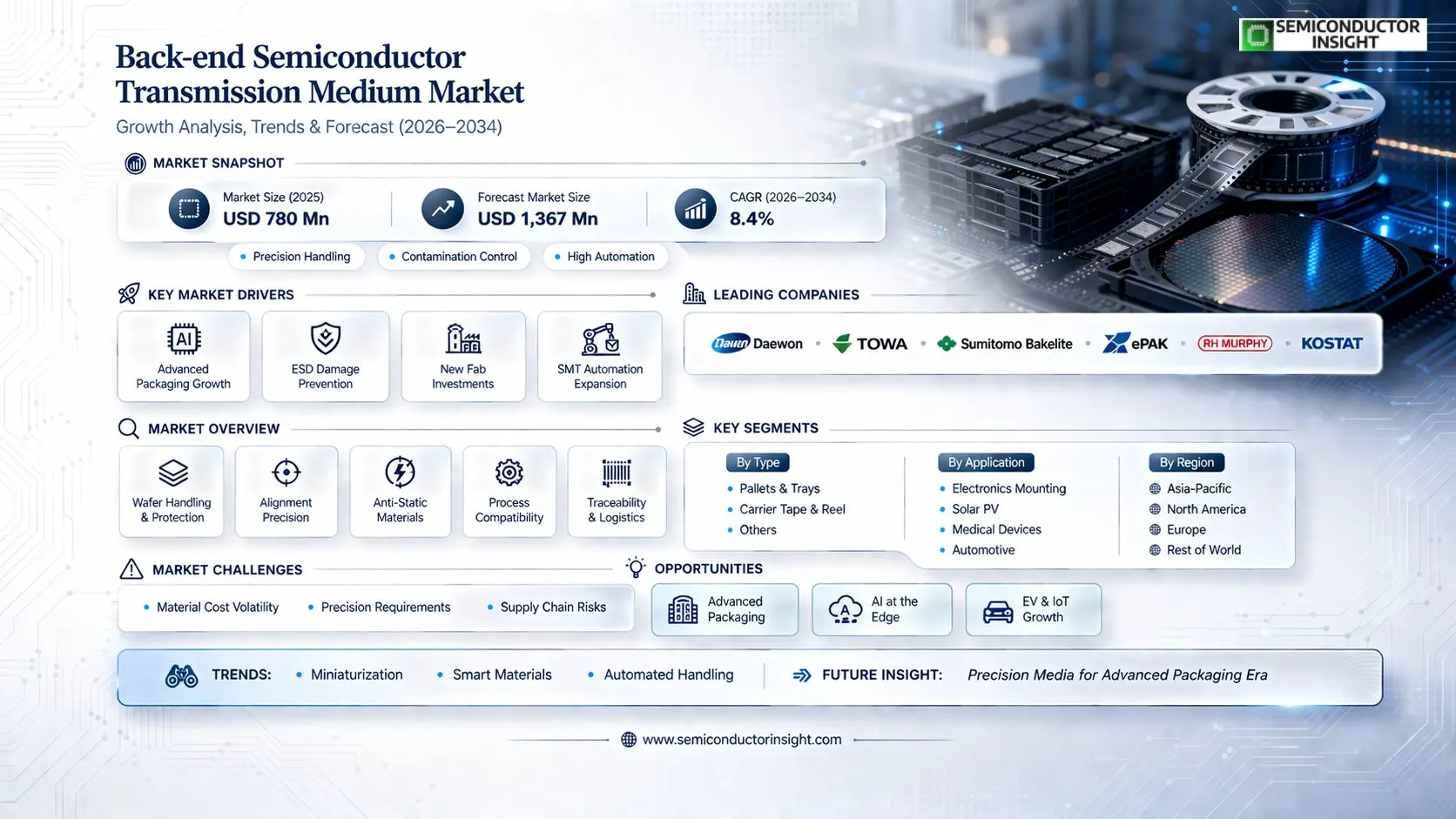
Global Back-end Semiconductor Transmission Medium market size was valued at USD 780 million in 2025. The market is projected to grow from USD 845 million in 2026 to USD 1,367 million by 2034, exhibiting a CAGR of 8.4% during the forecast period.
Back-end semiconductor transmission media are specialized carriers and handling solutions used in the final stages of semiconductor manufacturing. These critical components ensure the safe, stable, and precise placement of delicate semiconductor devices,such as integrated circuits (ICs), memory chips, and sensors,during assembly, testing, transportation, and final surface-mount technology (SMT) placement. The primary product categories include Pallets and Pallet-related Products, which provide rigid support for batches of wafers or packages; Carrier Tape and Reel systems, which are essential for automated component feeding into high-speed pick-and-place machines; and other specialized trays, magazines, and containers.
The market’s robust growth is fundamentally driven by the relentless expansion of Global electronics industry and increasing semiconductor complexity. As devices become smaller and more powerful,fueling demand in smartphones, automotive electronics, and Internet of Things (IoT) applications,the need for precision handling that prevents electrostatic discharge (ESD), physical damage, and contamination becomes paramount. Furthermore, significant investments in new semiconductor fabrication plants (fabs), particularly across regions like North America and Asia-Pacific under initiatives such as the U.S. CHIPS Act, are creating substantial demand for these back-end materials. Key industry players like Daewon, Towa Corporation, Sumitomo Bakelite, ePAK International Inc., RH Murphy Company Inc., KOSTAT Corporation etc., are continuously innovating with advanced polymers and designs to meet stringent industry standards for miniaturization and automation compatibility.
MARKET DRIVERS
Explosive Growth in AI and HPC Datacenters
The relentless demand for artificial intelligence training and high-performance computing is a primary catalyst. Advanced GPUs and AI accelerators require sophisticated back-end semiconductor transmission mediums to manage unprecedented data bandwidth and power delivery, pushing the adoption of advanced organic substrates and emerging glass core technologies.
Advanced Packaging and Heterogeneous Integration
Industry shifts toward 2.5D/3D IC packaging and chiplet architectures fundamentally reshape the market. This trend demands back-end semiconductor transmission medium solutions,such as silicon interposers and high-density substrates,that provide superior electrical interconnectivity and thermal management between disaggregated dies, directly enabling performance scaling beyond Moore’s Law.
➤ Global market for advanced packaging substrates, a core component of the back-end semiconductor transmission medium ecosystem, is projected to grow at a CAGR exceeding 14% over the next five years, driven by AI and automotive applications.
Furthermore, the proliferation of 5G/6G infrastructure and advanced automotive electronics creates sustained demand for robust, high-frequency packaging capable of reliable signal integrity, further cementing the critical role of transmission mediums in the semiconductor value chain.
MARKET CHALLENGES
Extreme Technical Complexity and Material Limitations
Developing next-generation back-end semiconductor transmission medium technologies involves significant hurdles. Achieving finer line/space features below 10 micrometers for higher interconnect density on organic substrates is increasingly difficult and costly. Simultaneously, managing thermomechanical stress and warpage in large, complex packages remains a persistent engineering challenge that can impact yield and reliability.
Other Challenges
Capital Intensity and Supply Chain Fragility
The manufacturing equipment for advanced substrates and interposers requires multibillion-dollar investments, creating high barriers to entry and concentrating supply among a few key players. This concentration, coupled with geopolitical tensions affecting material sourcing, introduces significant supply chain risks for the broader semiconductor industry.
Integration and Testing Bottlenecks
As packages become more complex, integrating disparate chiplets with different process nodes onto a single transmission medium demands new testing and Known-Good-Die (KGD) protocols. The lack of standardized interfaces and testing methodologies can slow time-to-market and increase overall system cost.
MARKET RESTRAINTS
High Development Costs and Extended Lead Times
The R&D and qualification cycles for novel back-end semiconductor transmission medium materials, such as glass cores or advanced laminates, are exceptionally long and capital-intensive. This high cost structure can deter adoption for mid-range applications, potentially restraining market expansion beyond the premium segment of AI and flagship mobile processors.
Intellectual Property and Design Ecosystem Hurdles
Success in chiplet-based design depends on a robust ecosystem of interoperable IP and design tools. Fragmentation in standards for the interfaces managed by the back-end semiconductor transmission medium can create vendor lock-in and design inertia, slowing the transition from traditional monolithic SoCs and acting as a market restraint.
MARKET OPPORTUNITIES
Adoption of Next-Generation Substrate Technologies
The commercial rollout of panel-level fan-out packaging and glass core substrates presents a significant growth vector. These technologies offer superior electrical performance and scalability for large, multi-chiplet packages compared to conventional organic substrates, creating a substantial opportunity for equipment and material suppliers in Back-end Semiconductor Transmission Medium market.
Expansion into Automotive and Edge AI
Beyond datacenters, the increasing semiconductor content in electric and autonomous vehicles requires high-reliability packaging solutions. Similarly, the deployment of AI at the edge in IoT devices creates demand for compact, power-efficient transmission mediums. These applications represent burgeoning markets with stringent requirements that drive innovation and value creation.
Material Innovation and Sustainability
There is a growing opportunity in developing novel, sustainable materials,such as bio-based polymers or advanced ceramics,for substrate cores and dielectric layers. Innovations that reduce environmental impact while improving performance or thermal dissipation can capture market share and align with broader industry ESG goals.
Back-end Semiconductor Transmission Medium Market Trends
Increasing Demand for Advanced Packaging Solutions
Back-end Semiconductor Transmission Medium market is directly influenced by Global shift towards advanced semiconductor packaging technologies like 2.5D/3D IC integration and fan-out wafer-level packaging. These complex packaging methodologies require exceptionally precise and reliable handling to prevent damage to delicate interconnects and micro-bumps. Consequently, manufacturers of transmission media such as specialized carrier tapes, precision pallets, and trays are innovating with anti-static, low-particulate, and dimensionally stable materials to meet the stringent cleanliness and tolerance requirements of these next-generation assembly processes. This trend is a primary driver for R&D investment within the back-end supply segment.
Other Trends
Material Innovation for Sustainability and Performance
A significant subtopic within market trends is the development of new material compositions for Back-end Semiconductor Transmission Medium products. There is a growing focus on engineering thermoplastics and composite materials that offer reduced warpage, higher temperature resistance for lead-free soldering processes, and improved recyclability. This shift aims to address both performance demands in high-throughput surface-mount technology (SMT) lines and increasing regulatory and corporate pressures for sustainable manufacturing practices. The transition from standard plastics to advanced, durable polymers extends product lifespan and reduces contamination risk.
Automation and Smart Manufacturing Integration
The rise of fully automated fabs and smart manufacturing is pushing the evolution of Back-end Semiconductor Transmission Medium market from passive carriers to integrated components of the material handling system. Trends include the incorporation of RFID tags, QR codes, and machine-readable identifiers directly into tapes and pallets. This enables precise tracking of component lots throughout the assembly and logistics chain, improving yield management, inventory control, and compatibility with Industry 4.0 frameworks. This integration is becoming critical for the automobile and medical device industries, where traceability is paramount.
Geographic Expansion of Supply Chains
Geopolitical and supply chain resilience concerns are prompting a regionalization of semiconductor manufacturing capacity, particularly in North America and Europe. This decentralization is creating new demand centers for Back-end Semiconductor Transmission Medium products, as new and expanded assembly and packaging facilities require localized, just-in-time supply of these critical consumables. Established manufacturers and suppliers are adjusting their distribution and production strategies to serve these emerging regional hubs, influencing competitive dynamics and logistics models within the market.
COMPETITIVE LANDSCAPE
Key Industry Players
A Specialty Market Driven by Precision and Supply Chain Integration
Back-end Semiconductor Transmission Medium market is a consolidated space defined by high technical expertise in materials science and precision manufacturing. Global top five players commanded a significant revenue share in 2025, indicating a competitive structure where established leaders like Daewon and Sumitomo Bakelite leverage their extensive material portfolios and manufacturing scale. These companies specialize in critical components such as pallet systems and carrier tape & reel, which are essential for the safe handling and automated assembly of sensitive semiconductors. Success hinges on deep integration with the broader semiconductor supply chain, strict compliance with industry cleanliness standards, and the ability to innovate with advanced polymers and engineered materials to meet evolving device miniaturization and throughput demands.
Beyond the dominant leaders, the market features a robust tier of specialized providers that secure significant niches. Companies such as ePAK and Towa Corporation are recognized for their advanced automation-compatible solutions, while RH Murphy Company and KOSTAT provide critical design and customization services. Other players like Hana Micron and TopLine have solidified positions by catering to specific regional markets or application segments, including the high-growth solar photovoltaic and automotive industries. This diverse ecosystem ensures that device manufacturers have access to tailored solutions, fostering competition based on technical support, product reliability, and just-in-time delivery capabilities essential for fab and OSAT operations.
List of Key Back-end Semiconductor Transmission Medium Companies Profiled
- Daewon
- DAINICHI SHOJI K.K.
- Hana Micron
- Towa Corporation
- Sumitomo Bakelite
- ePAK
- RH Murphy Company
- 3M
- KOSTAT
- TopLine
- Mishima Kosan Co.,Ltd.
- Chyang-yeou
- UBoT Holding Limited
- WaferChem
Segment Analysis:
| Segment Category | Sub-Segments | Key Insights |
| By Type |
|
Carrier Tape and Reel is a critical and leading segment, primarily due to its integral role in automated surface-mount technology (SMT) assembly lines. The precision engineering required for tape pockets and reel dimensions ensures safe handling and accurate feeding of sensitive components into high-speed pick-and-place machines. This format supports industry standardization and logistics efficiency, directly impacting manufacturing throughput. Furthermore, continuous innovation in materials to reduce electrostatic discharge and physical damage is a key driver for adoption across advanced semiconductor packaging. |
| By Application |
|
Electronic Component Mounting Industry stands as the dominant application, driven by the universal need for reliable component handling in PCB assembly. The expansion of consumer electronics, IoT devices, and communication infrastructure creates sustained, high-volume demand. This segment requires transmission media that offer exceptional cleanliness, dimensional stability, and compatibility with increasingly miniaturized and complex components. The trend towards heterogeneous integration and advanced packaging further elevates the technical requirements, making specialized carriers essential for yield protection and operational efficiency in this fast-paced manufacturing environment. |
| By End User |
|
Semiconductor Foundries & OSAT Providers are the primary end-users, as their operations encompass the entire back-end process from assembly and test to shipment. These facilities have the most stringent requirements for contamination control, traceability, and damage prevention during intra-facility transport. Their high-mix, high-volume production models create a continuous demand for robust and standardized transmission solutions. The competitive landscape among these providers intensifies focus on supply chain reliability and cost-effective, high-performance carrier solutions that can scale with production ramps. |
| By Material Composition |
|
Antistatic & Conductive Polymers represent the leading material segment, essential for safeguarding sensitive semiconductor devices from electrostatic discharge (ESD) which can cause latent or catastrophic failures. The shift towards more intricate and smaller node geometries increases vulnerability, making ESD protection a non-negotiable specification. Material innovation focuses on achieving the perfect balance of static-dissipative properties, mechanical strength, low particle generation, and thermal stability to withstand process environments, thereby directly influencing product reliability and factory yield rates. |
| By Function |
|
Transport & Logistics Carriers are the fundamental function segment, forming the backbone of the supply chain between manufacturing stages and facilities. Their design prioritizes stackability, durability for long-distance shipping, and compatibility with automated material handling systems. The growth of geographically dispersed supply chains, especially in Asia, amplifies the need for carriers that ensure component integrity against vibration, moisture, and physical shock during transit. This segment’s evolution is closely tied to global trade patterns and the just-in-time delivery requirements of modern electronics manufacturing. |
Regional Analysis: Back-end Semiconductor Transmission Medium Market
Asia-Pacific
Taiwan’s OSAT giants and South Korea’s integrated device manufacturers (IDMs) are at the forefront of developing and commercializing the most complex Back-end Semiconductor Transmission Medium systems. Their focus is on enabling heterogeneous integration for AI chips, pushing the boundaries of TSV density and microbump pitch to achieve superior performance and bandwidth in a compact form factor. Their technological roadmaps directly shape global standards.
China is aggressively expanding its domestic Back-end Semiconductor Transmission Medium capabilities to achieve supply chain self-sufficiency, heavily investing in advanced substrate and packaging R&D. Meanwhile, Southeast Asia (Malaysia, Vietnam) serves as a crucial manufacturing base for volume production of established packaging technologies and related interconnect media, offering cost advantages and geographic diversification for global supply chains.
The region’s leadership is solidified by a fully integrated ecosystem. Proximity between leading substrate suppliers, specialty chemical providers, and OSAT facilities enables rapid prototyping, collaborative problem-solving, and swift scaling of new Back-end Semiconductor Transmission Medium solutions. This tight integration drastically reduces time-to-market for advanced packaging platforms.
Surging demand from Asia-Pacific-based technology leaders in consumer electronics, telecommunications, and computing creates a powerful local pull. This drives continuous innovation in Back-end Semiconductor Transmission Medium, as packaging and interconnect solutions are co-developed to meet the specific power, performance, and miniaturization needs of next-generation regional end-products.
North America
North America, led by the United States, functions as the primary center for the design, architecture definition, and R&D for cutting-edge Back-end Semiconductor Transmission Medium technologies. While manufacturing scale is smaller, the region’s strength lies in its semiconductor intellectual property (IP), Electronic Design Automation (EDA) tools, and innovative materials science. Major fabless design companies and integrated device manufacturers (IDMs) based in the U.S. set the architectural requirements that drive developments in interconnects, substrates, and packaging schemes. This creates a strong demand-pull for highly specialized, performance-driven transmission media. Collaborative research between national labs, academia, and industry focuses on novel materials and integration schemes, positioning North America as the conceptual leader defining the future roadmap for Global Back-end Semiconductor Transmission Medium Market.
Europe
Europe maintains a specialized and influential role in Back-end Semiconductor Transmission Medium market, centered on precision engineering, high-reliability applications, and advanced materials research. The region excels in supplying highly specialized equipment used to manufacture advanced interconnect structures, such as lithography and plating tools for creating fine-pitch redistribution layers. European expertise is critical for market segments requiring extreme reliability, such as automotive (particularly for electric and autonomous vehicles) and industrial applications. Here, the focus for transmission media is on thermal management, long-term durability under harsh conditions, and integration with power semiconductors. Collaborative European Union initiatives and strong academic institutions drive R&D in new material interfaces and sustainable manufacturing processes for these critical back-end components.
South America
The South American market for Back-end Semiconductor Transmission Medium is currently nascent but exhibits potential for growth as a focused manufacturing and assembly hub for specific applications. The region’s involvement is primarily through the operation of back-end semiconductor assembly and test facilities, which serve both local consumer electronics markets and global supply chains seeking geographic diversification. Investment is gradually increasing in infrastructure to support more sophisticated packaging operations. Market dynamics are driven by local demand from telecommunications infrastructure upgrades and automotive manufacturing, which create a foundational need for reliable, cost-effective semiconductor packaging and the associated transmission media. Strategic partnerships with technology providers from leading regions are key to transferring expertise and building a more substantial local capability over the long term.
Middle East & Africa
The Middle East & Africa region represents an emerging and strategic growth frontier for Back-end Semiconductor Transmission Medium market. Significant sovereign investments, particularly in nations like Saudi Arabia and the UAE, are being channeled into building a foundational semiconductor ecosystem with a stated focus on advanced packaging and assembly. These long-term initiatives aim to create regional hubs for back-end manufacturing, which would inherently require the establishment of supply chains for substrates and interconnect materials. While current capabilities are limited, the strategic vision involves attracting international OSAT partners and leveraging investments in adjacent sectors like data centers and smart infrastructure to cultivate future demand for localized, high-performance semiconductor packaging solutions.
Report Scope
This market research report provides a comprehensive analysis of the Back-end Semiconductor Transmission Medium Market , covering the forecast period 2026–2034. It offers detailed insights into market dynamics, technological advancements, competitive landscape, and key trends shaping the industry.
Key focus areas of the report include:
- Market Overview: The report begins with an overview outlining its current market scenario, key growth indicators, and industry transformation drivers. It discusses macroeconomic factors, demand–supply balance, regulatory landscape, and the strategic role of semiconductors in powering advancements across industries such as automotive, telecommunications, consumer electronics, and industrial automation.
- Market Size & Forecast: Historical data and future projections for revenue, unit shipments, and market value across major regions and segments.
- Segmentation Analysis: Detailed breakdown by product type, technology, application, and end-user industry to identify high-growth segments and investment opportunities.
- Regional Insights: Insights into market performance across North America, Europe, Asia-Pacific, Latin America, and the Middle East & Africa, including country-level analysis where relevant.
- Competitive Landscape: Profiles of leading market participants, including their product offerings, R&D focus, manufacturing capacity, pricing strategies, and recent developments such as mergers, acquisitions, and partnerships.
- Technology Trends & Innovation: Assessment of emerging technologies, integration of AI/IoT, semiconductor design trends, fabrication techniques, and evolving industry standards.
- Market Drivers & Restraints: Evaluation of factors driving market growth along with challenges, supply chain constraints, regulatory issues, and market-entry barriers.
- Stakeholder Insights: Insights for component suppliers, OEMs, system integrators, investors, and policymakers regarding the evolving ecosystem and strategic opportunities.
Primary and secondary research methods are employed, including interviews with industry experts, data from verified sources, and real-time market intelligence to ensure the accuracy and reliability of the insights presented.
FREQUENTLY ASKED QUESTIONS:
What is the current market size of Back-end Semiconductor Transmission Medium Market?
-> Global Back-end Semiconductor Transmission Medium Market was valued at USD 780 million in 2025 and is projected to reach USD 1367 million by 2034, growing at a CAGR of 8.4% during the forecast period.
Which key companies operate in Back-end Semiconductor Transmission Medium Market?
-> Key players include Daewon, DAINICHI SHOJI K.K., Hana Micron, Towa Corporation, Sumitomo Bakelite, ePAK, RH Murphy Company, 3M, KOSTAT, and TopLine, among others.
What are the key growth drivers?
-> The market is driven by rising demand for semiconductors across various industries and the critical need for safe, stable, and precise handling of components during manufacturing, transportation, and assembly operations.
Which region dominates the market?
-> The U.S. and Chinese markets represent significant national markets within Global landscape. Regionally, Asia is a key region for the semiconductor industry and its supporting supply chain.
What are the key market segments?
-> The market is segmented by type into Pallets and Pallet-related Products, Carrier Tape and Reel, and Others. By application, key segments include the Electronic Component Mounting Industry, Solar Photovoltaic Industry, Medical Device Industry, and Automobile Industry.

Get Sample Report PDF for Exclusive Insights
Report Sample Includes
- Table of Contents
- List of Tables & Figures
- Charts, Research Methodology, and more...
 Download Sample Report PDF