Key Statistics
Key Takeaways
- FFKM seals occupy the highest-performance end of the market because plasma, fluorine chemistry, elevated temperature and vacuum exposure make material purity and service life more valuable than unit price in critical chamber locations.
- Etching and deposition equipment is the most demanding process environment, where seal performance directly influences particles, maintenance intervals and chamber availability.
- Asia Pacific remains the market center because Taiwan, South Korea, China and Japan carry the highest concentration of wafer-fabrication capacity and equipment installations.
- Fab-equipment investment is a direct demand multiplier. SEMI’s 3Q 2026 outlook places global 300mm front-end equipment spending at USD 149 billion in 2026, supporting seal consumption across new tools and installed-base maintenance.
- Qualification depth is the core competitive barrier. Semiconductor-grade seals are purchased on process compatibility, contamination control, validated lifetime and supply consistency rather than commodity elastomer pricing.
Semiconductor Seals Market Overview
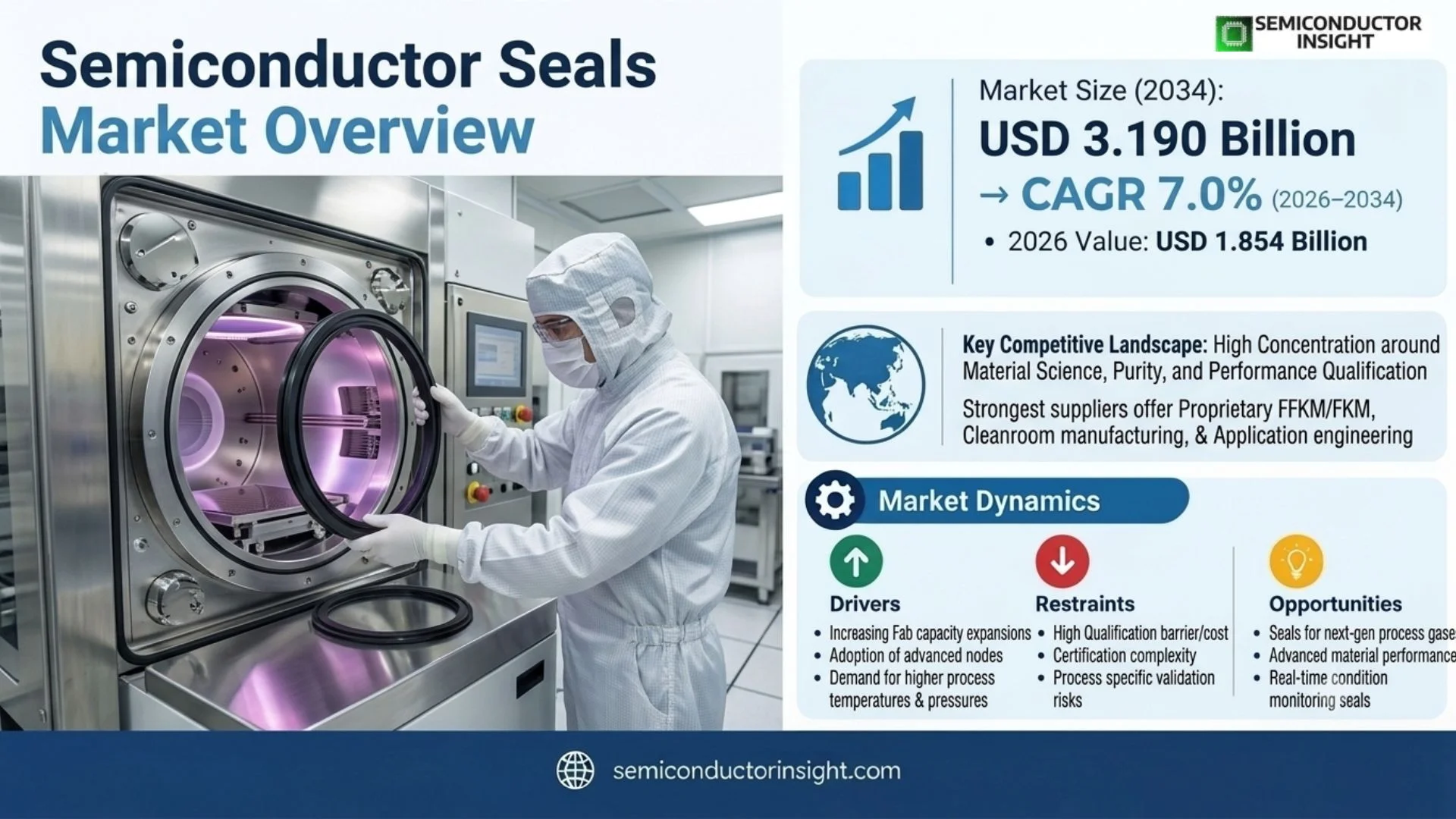
Semiconductor Seals Market was valued at USD 1.732 billion in 2025. The market is estimated at USD 1.854 billion in 2026 and is projected to reach USD 3.190 billion by 2034, expanding at a CAGR of 7.0% during 2026–2034. Asia Pacific remains the largest regional market.
Semiconductor seals are engineered O-rings, gaskets and custom sealing components installed throughout wafer-fabrication tools, subfab systems and chemical delivery equipment. Their role is to maintain vacuum integrity, isolate aggressive process gases and liquids, limit particles and metal contamination, and protect moving or static interfaces during repeated thermal and pressure cycling. The market therefore sits inside the semiconductor equipment maintenance and consumables chain rather than the broader industrial sealing market, with qualification requirements that are specific to process chemistry, tool architecture and cleanliness class.
Material choice is application-specific. FKM remains economically attractive in less aggressive locations, while FFKM is favored where plasma exposure, fluorinated chemistries, high temperature and low outgassing make premature failure expensive. PTFE and engineered thermoplastics also appear in spring-energized and custom sealing geometries. DuPont’s Kalrez semiconductor selector describes perfluoroelastomer parts formulated for aggressive wafer-processing environments, while Trelleborg and Greene Tweed position high-purity FFKM and FKM compounds around plasma, thermal, wet-clean and deposition applications.
Demand is linked to tool count, process intensity and maintenance cycles. SEMI’s Q3 2026 300mm Fab Outlook projects record front-end fab equipment spending of USD 149 billion in 2026 and a 7% increase in installed 300mm capacity during the year. More chambers, tighter process windows and higher uptime targets increase both original-equipment seal content and replacement consumption. This makes semiconductor seals a recurring consumables market whose revenue grows with fab capacity, process complexity and the installed base of etch, deposition, cleaning and vacuum systems.
Segment Analysis: By Type
By material type, the market is segmented into FFKM, FKM, FVMQ, VMQ and other sealing materials. FKM is widely used where chemical and temperature requirements are moderate, while FFKM carries the strongest position in high-value plasma, deposition and hot-process locations because its chemical resistance and purity reduce failure risk and unplanned chamber intervention.
| Type | Technical / commercial role | Market position |
|---|---|---|
| FFKM | Perfluoroelastomer used in aggressive plasma, fluorine chemistry, high-temperature and high-vacuum locations. | Highest-value material class; favored where seal life, purity and chemical compatibility outweigh acquisition cost. |
| FKM | Fluoroelastomer for less severe chemical and thermal locations, subfab systems and cost-sensitive tool positions. | Broad installed base and strong volume position; competes on formulation quality, cleanliness and total cost of ownership. |
| FVMQ | Fluorosilicone-based sealing material used where fuel, solvent and low-temperature behavior matter. | Niche semiconductor use; selected for specific chemical and flexibility requirements rather than broad chamber exposure. |
| VMQ | Silicone elastomer for temperature flexibility and selected low-stress sealing locations. | Smaller process-tool role because plasma and aggressive chemistry resistance is below FFKM/FKM levels. |
| Others | PTFE-based, engineered thermoplastic and specialty composite sealing solutions. | Important in spring-energized seals, wafer handling, valve interfaces and custom geometries where elastomers alone are insufficient. |
Product form and performance-grade segmentation
Product form changes the commercial and qualification pathway. O-rings dominate standardized static and dynamic interfaces, while gaskets and custom seals are more design-specific and can remain tied to a particular tool platform for years. Performance grade adds another layer: high-purity and low-outgassing parts command stronger value in advanced-node chambers because particle generation, extractables and trace-metal contamination are closely controlled. Cleanroom production, validated washing and packaging, and lot traceability therefore become part of the product rather than post-production services.
| Axis | Segments | Commercial significance |
|---|---|---|
| By Product Type | O-rings; Gaskets & Seals | O-rings support repeatable high-volume replacement; custom gaskets and engineered seals carry more design-lock and qualification value. |
| By Performance Grade | Standard-grade; High-purity / Low-outgassing | High-purity grades are selected for the most contamination-sensitive chamber and gas-path locations, supporting higher pricing and longer qualification cycles. |
Segment Analysis: By Application
By application, the market is segmented into plasma processing, hot processing and wet chemical processing. Plasma processing is the most demanding application because oxygen, fluorine and other reactive species can rapidly attack conventional elastomers, while hot processing raises compression-set and thermal-stability requirements and wet chemistry places chemical compatibility at the center of material selection.
| Application | Demand characteristics |
|---|---|
| Plasma Processing | Etch and plasma-clean chambers require low particle generation, plasma resistance and stable sealing under repeated exposure. FFKM is strongly positioned in critical locations, and supplier qualification commonly includes application-specific plasma and cycling tests. |
| Hot Processing | Thermal treatment, CVD and other elevated-temperature steps demand low compression set, vacuum stability and resistance to temperature cycling. Seal failure carries high downtime cost, supporting premium compounds where service life is demonstrably longer. |
| Wet Chemical Processing | Cleaning, chemical delivery and wet benches expose seals to acids, solvents and oxidizers. Material compatibility, extractables and dimensional stability determine selection, with FKM, FFKM, PTFE and engineered plastics used according to chemistry and temperature. |
Segment Analysis: By Process Application
Process application separates seals by the tool function in which they are installed. Etching and deposition equipment has the strongest performance burden because process chambers combine vacuum, plasma, elevated temperature and reactive gases. Cleaning and gas-delivery systems emphasize chemical resistance, contamination control and reliable valve or line isolation. Both groups generate recurring replacement demand as seal lifetime is managed through preventive-maintenance schedules.
| Process Application | Demand profile |
|---|---|
| Etching & Deposition Process Seals | High-value, qualification-intensive locations where uptime and particle control support premium FFKM and engineered sealing solutions. |
| Cleaning & Gas Delivery System Seals | High-volume chemical-contact applications where compatibility, purity and leak prevention are central purchasing criteria. |
Segment Analysis: By End User
The end-user base includes front-end equipment manufacturers, fab operators and research laboratories. Equipment OEMs influence initial material and geometry qualification, while fab operators drive aftermarket replacement and increasingly co-qualify alternative materials to manage lifetime, supply continuity and cost. Research laboratories represent a smaller but technically demanding segment because pilot tools often expose seals to non-standard chemistries and process conditions.
| End User | Purchasing role |
|---|---|
| Front-end Equipment Manufacturers | Define original specifications, drawing controls and approved materials for new tool platforms. |
| Fab Operators | Drive recurring replacement demand, preventive-maintenance schedules and alternative-material qualification. |
| Research Laboratories | Require small-volume, high-specification seals for pilot tools, process development and non-standard conditions. |
Regional Analysis
Asia Pacific leads the semiconductor seals market because it contains the largest concentration of front-end semiconductor capacity and equipment installations. North America is gaining strategic importance as new fabs and equipment-supply investments expand, while Europe remains a high-specification market anchored by lithography, automotive, power semiconductor and equipment ecosystems.
How does regional demand differ across the semiconductor seals market?
Regional demand follows the geography of wafer fabrication, but commercial requirements differ. Asia Pacific emphasizes local engineering support, short lead times and high-volume replenishment around dense fab clusters. North America combines legacy installed-base demand with new-fab localization and supply-security priorities. Europe places a strong premium on traceability, specialty materials and equipment-linked qualification. South America and Middle East & Africa remain much smaller and are served mainly through global distributors and OEM-linked supply chains.
| Region | Position | Growth outlook | Demand profile | Commercial selection factor |
|---|---|---|---|---|
| Asia Pacific | Largest | High | New fabs + installed-base maintenance | Local availability, technical support, cleanliness and qualification |
| North America | Strategic growth market | High | New-fab localization + replacement | Qualified materials, supply resilience and OEM/fab approvals |
| Europe | High-specification niche | Moderate | Equipment ecosystem + automotive/power fabs | Purity, traceability, compliance and specialized engineering |
| South America | Small | Selective | Imported equipment maintenance | Distributor coverage and landed cost |
| Middle East & Africa | Emerging | Selective | Technology investment + imported tools | Supply reliability and technical support |
Key Semiconductor Seals Manufacturers and Competitive Landscape
Competition is concentrated around material science, process qualification and global support rather than simple molding scale. The strongest suppliers combine proprietary FFKM/FKM formulations, cleanroom manufacturing, application engineering and local support near major fabs and equipment OEMs. Once a material is qualified in a chamber location, switching carries validation cost and process risk, which creates durable positions for suppliers that can document purity, particle performance and lifetime.
DuPont’s Kalrez franchise is positioned around perfluoroelastomer parts formulated for aggressive semiconductor wafer-processing environments, including plasma processes. Trelleborg offers Isolast PureFab FFKM, high-purity FKM and PTFE-based solutions supported by cleanroom manufacturing and semiconductor-dedicated facilities. Greene Tweed competes through Chemraz FFKM, Fusion FKM and engineered components for etch, deposition, wet cleaning and advanced packaging. These product families illustrate how the premium tier competes on application-specific performance rather than catalog breadth alone.
Japanese and Asian suppliers such as NOK, Eagle Industry, Daikin, VALQUA and other specialist seal manufacturers benefit from proximity to the region’s large equipment and fab base. Their competitive advantage is strongest where local qualification support, rapid replenishment and joint development with equipment makers are required. Smaller specialists can still hold defensible positions in legacy tools or narrow chemistries when they possess a validated compound, geometry or customer approval that is difficult to replace.
Supply continuity has become more important as fabs seek resilience in maintenance-critical consumables. Trelleborg’s 2026 Malta expansion explicitly links added European FKM/FFKM cleanroom capacity to shorter lead times and business continuity. Similar localization decisions reinforce a market structure in which global suppliers add regional manufacturing or stocking while preserving centralized material-development expertise.
Tier structure
| Competitive tier | Representative companies | How they compete |
|---|---|---|
| Global high-performance material and sealing specialists | DuPont, Trelleborg, Greene Tweed, Parker, Saint-Gobain, Freudenberg | Proprietary materials, semiconductor cleanroom processes, global technical support and deep qualification history. |
| Asia-based semiconductor sealing specialists | NOK Corporation, Eagle Industry, Daikin, VALQUA, Applied Seals, MNE | Regional proximity, tool-OEM relationships, rapid response and semiconductor-specific product breadth. |
| Specialized / regional suppliers | Precision Polymer Engineering (IDEX), Vulcan Seals, Maxmold Polymer and other profiled firms | Custom geometries, legacy-tool support, niche materials or regional service. |
Key companies profiled
Dupont, NOK Corporation, Eagle Industry, Parker, Daikin, VALQUA, Trelleborg, Applied Seals, Saint-Gobain, Precision Polymer Engineering (IDEX), MNE Co., Ltd, Freudenberg, Greene Tweed, Vulcan Seals, Maxmold Polymer, Ceetak, MITSUBISHI CABLE INDUSTRIES, GMORS, MFC Sealing Technology, IC SEAL, Northern Engineering (Sheffield) Ltd, Sigma Seals & Gaskets, AIR WATER MACH
Semiconductor Seals Production Capacity Analysis
Production capacity in semiconductor seals is not measured only by molding tonnage. The binding capacity is qualified cleanroom output in the correct material, geometry and process window. Compound preparation, molding, post-cure, washing, inspection and contamination-controlled packaging all become capacity constraints when parts are destined for advanced wafer-processing tools. A supplier can possess general elastomer capacity yet still be unable to serve a semiconductor program if the required compound, cleanroom, traceability or validation system is absent.
Trelleborg states that it has more than 35 manufacturing facilities worldwide and identifies six sites specifically dedicated to developing, testing or producing advanced semiconductor sealing solutions. Its Malta expansion added more than 500 square meters of cleanroom space focused on FKM and FFKM, while its semiconductor network also includes dedicated capabilities in the United Kingdom, South Korea, Germany and the United States. This distributed model reduces the supply risk associated with a single qualified plant.
Upstream risk sits in high-purity fluoropolymer and specialty elastomer feedstocks as well as compounding know-how. FFKM is technically demanding and expensive to formulate and process, so capacity additions require more than standard rubber-molding equipment. Downstream, the qualification cycle itself can delay usable capacity: new compounds or production sites may need customer testing before they can substitute for an incumbent seal in a contamination-sensitive chamber.
| Capacity factor | Market implication |
|---|---|
| Semiconductor-dedicated cleanrooms | Limits the number of facilities that can produce washed, packed and traceable parts for critical tool locations. |
| Proprietary FFKM/FKM compounding | Creates material differentiation and constrains rapid capacity replication. |
| Application testing and plasma validation | Determines whether nominal production capacity can become qualified commercial supply. |
| Regional manufacturing and stocking | Reduces lead-time and continuity risk for maintenance-critical consumables. |
Semiconductor Seals Market Dynamics: Drivers, Restraints and Opportunities
Growth is driven by expanding fab capacity, rising process complexity and the recurring replacement nature of seals, while restraints come from long qualification cycles, high-performance material cost and the need to prove contamination behavior under increasingly severe process conditions. The strongest opportunities are in advanced-node plasma environments, regionalized supply and lower-impact material systems that preserve semiconductor-grade performance.
MARKET DRIVERS
Drivers Impact Analysis*
| Driver | Relative impact on growth | Commercial mechanism |
|---|---|---|
| 300mm fab equipment and capacity growth | High | More chambers and tools increase original-equipment seal content and the installed base requiring replacement. |
| Advanced process severity | High | Higher plasma power, aggressive chemistries and tighter contamination limits raise demand for premium FFKM and engineered seals. |
| Preventive maintenance and uptime economics | Medium-High | Longer seal life reduces chamber downtime, making total cost of ownership more important than unit price. |
| Regional supply localization | Medium | Fabs and OEMs reward qualified local production and shorter replenishment cycles. |
Record front-end equipment investment expands the installed base
SEMI’s Q3 2026 300mm Fab Outlook projects global 300mm front-end fab equipment spending of USD 149 billion in 2026, up 31% year over year, and a 7% increase in installed 300mm capacity. Every new etch, deposition, clean, thermal and vacuum tool adds sealing interfaces that require original fitment and later replacement. Because seals are maintenance consumables rather than one-time capital components, the installed-base effect persists for years after equipment is commissioned.
Advanced-node process conditions raise seal value per chamber
Shrinking geometries and increasingly complex process stacks tighten limits on particles, extractables and metal contamination. Plasma chemistries and higher thermal loads can shorten the life of conventional elastomers, making FFKM and engineered sealing solutions economically attractive where a longer maintenance interval protects expensive chamber availability. This shifts market mix toward higher-purity, process-specific materials even when total seal unit volumes grow at a slower rate than equipment spending.
Local support and qualification deepen supplier integration
Seal selection is often tied to tool design, process chemistry and maintenance procedures, so suppliers that can work directly with OEM and fab engineers gain an advantage. Local application laboratories, cleanroom production and inventory shorten development and replenishment cycles. The same dynamic raises switching costs because a substitute must demonstrate equivalent particle, chemical and lifetime behavior before a fab will accept it in a critical chamber location.
MARKET RESTRAINTS
Restraints Impact Analysis*
| Restraint | Relative impact on growth | Commercial mechanism |
|---|---|---|
| Long qualification and change-control cycles | High | Alternative materials can take months of testing before approval, slowing supplier switching and new-product adoption. |
| FFKM and specialty-material cost | Medium-High | High-performance elastomers raise part cost and encourage use of FKM or engineered alternatives in less severe locations. |
| Process-specific fragmentation | Medium | Different chemistries and tool platforms prevent one compound from serving every application, increasing SKU and testing complexity. |
| Fluorinated-material regulatory pressure | Medium | PFAS-related policy and customer sustainability goals can raise reformulation and documentation requirements. |
Qualification cycles slow commercialization
A semiconductor seal must perform in the customer’s actual chemistry, temperature, vacuum and motion conditions while meeting contamination limits. Even a technically strong material may require extended lab and tool testing before approval, particularly when it replaces an incumbent part. This limits the speed at which new suppliers can scale and means announced production capacity does not immediately translate into market share.
Premium materials carry substantial cost
FFKM delivers strong chemical and thermal resistance but is materially more expensive than conventional FKM and silicone families. Fab operators therefore optimize by location, using premium materials only where failure consequences justify the cost. This caps FFKM penetration in utility, subfab and less aggressive positions and preserves demand for lower-cost qualified materials.
Regulatory pressure on fluorinated materials raises development burden
The sealing industry is developing alternatives and lower-impact formulations as customers and regulators scrutinize fluorinated substances. Trelleborg reported launching its first PFAS-free elastomer for demanding semiconductor applications during 2025. Transitioning such materials into semiconductor tools still requires the same purity, lifetime and chemistry validation as incumbent products, so regulatory-driven innovation can initially add cost and qualification work.
MARKET OPPORTUNITIES
Advanced-node plasma and deposition tools
The most attractive opportunity is at chamber locations where aggressive plasma, high temperature and contamination control make seal failure costly. Suppliers that can prove longer service life or lower particle generation can capture premium value and become designed-in on future tool generations.
Regionalized qualified capacity
Fabs increasingly value continuity and shorter lead times for maintenance consumables. Expanding cleanroom molding, washing and packaging near major semiconductor clusters allows suppliers to reduce logistics risk while preserving centralized material development. Trelleborg’s Malta expansion is a direct example of this strategy in Europe.
PFAS-free and lower-impact high-performance compounds
Semiconductor customers want environmental improvements without sacrificing plasma resistance, purity or lifetime. Suppliers able to qualify PFAS-free or reduced-impact elastomers for demanding processes can open a new replacement cycle and strengthen relationships with sustainability-focused OEMs and fabs.
Data-driven predictive maintenance
Seal life is increasingly evaluated as part of chamber uptime rather than as a component purchase. Suppliers that combine materials expertise with condition data, failure analysis and application engineering can move from selling parts to managing sealing performance, improving retention and increasing value per customer.
Semiconductor Seals Supply Chain Analysis
High-purity polymer and specialty feedstocks
Compound formulation and cleanroom molding
Cleaning, inspection, packaging and qualification
OEM/fab installation, maintenance and replacement
At the upstream stage, high-purity fluorinated polymers, curing systems, fillers and engineered thermoplastics determine the achievable chemical resistance, outgassing and contamination profile. The formulation is a major source of intellectual property, particularly for FFKM compounds designed for plasma and high-temperature service. Feedstock quality and continuity therefore influence both performance and the ability to reproduce a qualified material across manufacturing sites.
Manufacturing combines compounding, molding or machining, post-cure and tight dimensional control. Semiconductor production adds cleanroom handling, washing and packaging that are not required for ordinary industrial seals. Trelleborg’s cleanroom facilities describe ISO Class 7 production with separate ISO Class 5 cleaning and packaging for relevant components, illustrating why semiconductor capacity must be viewed as a controlled process chain rather than basic molding output.
Qualification connects manufacturing to commercial value. OEMs and fabs validate the material, geometry and production process for a specific tool location. Once approved, replacement demand flows through preventive maintenance, spare-parts programs and direct fab purchasing. The result is a supply chain with relatively small component values but high switching costs because an unproven seal can create contamination, leakage or downtime far exceeding the purchase price.
Recent Developments in the Semiconductor Seals Market
24 Aug 2026 – Trelleborg expands Malta semiconductor production center
Trelleborg announced an expanded European production center with more than 500 square meters of added cleanroom space focused on FKM and FFKM products. The company linked the investment to shorter lead times, business continuity and greater regional manufacturing support for semiconductor customers. Source
2 Mar 2026 – Trelleborg highlights PFAS-free semiconductor elastomer
Trelleborg Sealing Solutions reported that one of its major 2025 achievements was the launch of its first PFAS-free elastomer for demanding semiconductor applications, alongside expanded Malta cleanroom capacity. This signals active material reformulation as environmental requirements rise. Source
2025 – DuPont documents semiconductor low-permeation Kalrez seals
DuPont’s 2025 sustainability reporting highlighted Kalrez low-permeation seals designed for high-temperature and high-vacuum semiconductor manufacturing conditions. The development reinforces the shift toward application-specific sealing materials tied to advanced process requirements. Source
REPORT SCOPE & SEGMENTATION
| Report Title | Semiconductor Seals Market Size, Share & Industry Analysis, By Type (FFKM, FKM, FVMQ, VMQ, Others), By Product Type (O-rings, Gaskets & Seals), By Performance Grade (Standard-grade Semiconductor Seals, High-purity / Low-outgassing Semiconductor Seals), By Process Application (Etching & Deposition Process Seals, Cleaning & Gas Delivery System Seals), By Application (Plasma Processing, Hot Processing, Wet Chemical Processing), and Regional Forecast, 2026-2034 |
| Base / Estimated / Forecast Years | 2025 / 2026 / 2034 |
| Market Size | USD 1.732 billion in 2025; USD 1.854 billion in 2026; USD 3.190 billion by 2034 |
| Forecast CAGR | 7.0% during 2026–2034 |
| Regional Coverage | North America, Europe, Asia Pacific, South America, Middle East & Africa |
| By Type | FFKM; FKM; FVMQ; VMQ; Others |
| By Product Type | O-rings; Gaskets & Seals |
| By Performance Grade | Standard-grade Semiconductor Seals; High-purity / Low-outgassing Semiconductor Seals |
| By Process Application | Etching & Deposition Process Seals; Cleaning & Gas Delivery System Seals |
| By Application | Plasma Processing; Hot Processing; Wet Chemical Processing |
| By End User | Front-end equipment manufacturers; Fab operators; Research laboratories |
| Key Companies Profiled | Dupont, NOK Corporation, Eagle Industry, Parker, Daikin, VALQUA, Trelleborg, Applied Seals, Saint-Gobain, Precision Polymer Engineering (IDEX), MNE Co., Ltd, Freudenberg, Greene Tweed, Vulcan Seals, Maxmold Polymer, Ceetak, MITSUBISHI CABLE INDUSTRIES, GMORS, MFC Sealing Technology, IC SEAL, Northern Engineering (Sheffield) Ltd, Sigma Seals & Gaskets, AIR WATER MACH |
Frequently Asked Questions
What is the current size of the semiconductor seals market?
The global semiconductor seals market is estimated at USD 1.732 billion in 2025, rising to USD 1.854 billion in 2026 and projected to reach USD 3.190 billion by 2034, representing a 7.0% CAGR during 2026–2034.
Which materials are most important in semiconductor seals?
FFKM and FKM are the principal elastomer families. FFKM is selected for the harshest plasma, chemical and high-temperature chamber locations, while FKM serves less severe applications where a lower material cost can meet the required chemical resistance and cleanliness.
Which applications generate the strongest demand?
Plasma processing, hot processing and wet chemical processing are the core application groups. Etch and deposition chambers are especially demanding because seals face vacuum, reactive gases, plasma exposure and contamination limits that can directly affect chamber uptime and wafer yield.
Which region leads the semiconductor seals market?
Asia Pacific leads because Taiwan, South Korea, China and Japan contain the highest concentration of semiconductor fabrication capacity and process equipment. The region therefore has the largest installed base for both original-equipment seals and recurring replacement demand.
What is driving market growth through 2034?
The main drivers are expanding 300mm fab capacity, record front-end equipment investment, more severe process conditions at advanced nodes, preventive-maintenance demand and the need for qualified regional supply. These forces raise both seal unit consumption and the value of high-performance materials.
What constrains adoption of new seal suppliers?
Qualification is the principal barrier. New materials and production sites must prove chemical compatibility, dimensional stability, low contamination and reliable lifetime in the relevant tool location. That validation cycle slows switching even when an alternative material offers a lower purchase price.
Who are the key semiconductor seal suppliers?
The profiled company set includes Dupont, NOK Corporation, Eagle Industry, Parker, Daikin, VALQUA, Trelleborg, Applied Seals, Saint-Gobain, Precision Polymer Engineering (IDEX), MNE, Freudenberg, Greene Tweed, Vulcan Seals and other specialist suppliers.
What opportunities are emerging in semiconductor sealing?
High-value opportunities include advanced plasma and deposition seals, PFAS-free or lower-impact materials, regional cleanroom production near fab clusters, and performance programs that use application engineering and failure analysis to extend maintenance intervals.
Research Sources & Evidence Base
Get Sample Report PDF for Exclusive Insights
Report Sample Includes
- Table of Contents
- List of Tables & Figures
- Charts, Research Methodology, and more...