Key Statistics
Key Takeaways
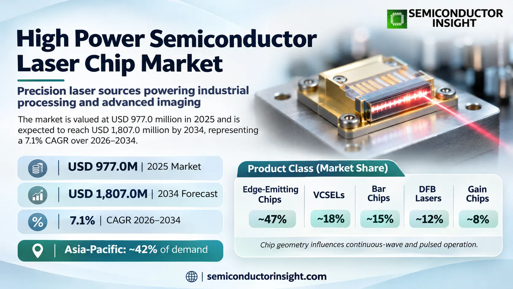
- Global trajectory: The international market for high-power semiconductor laser chips advances from USD 977.0 million in 2025 toward USD 1,807.0 million by 2034, a 7.1% annual rate. Industrial optical pumping, direct-material processing and precision sensing provide different purchase cycles that moderate reliance on any one end use.
- Emitter architecture: Edge-Emitting Chips account for an estimated ~47% of revenue, with VCSELs ~18%, Bar Chips ~15%, DFB Lasers ~12% and Gain Chips ~8%. High-output laser-diode chips compete through optical efficiency, wavelength stability, thermal control and lifetime rather than a simple count of emitted beams.
- Application structure: Industrial Pumping represents around ~43% of market demand, followed by Medical & Aesthetic Devices near ~20%, Automotive LiDAR & 3-D Sensing ~16%, Projection & High-Brightness Displays ~13%, and Scientific Instrumentation ~8%. Different wavelength and packaging requirements create distinct qualification pathways for each.
- Regional balance: Asia-Pacific generates an estimated ~42% of semiconductor laser chip revenue, Europe ~25% and North America ~23%. The Middle East and Africa add approximately ~6%, with South and Central America at ~4%. Epitaxy and optical packaging clusters do not necessarily coincide with the site where a complete laser system is installed.
- Production constraints: Facet degradation, wafer epitaxy consistency and thermal cycling remain critical risks, especially for sustained high optical power. TRUMPF describes unmounted 790–1100 nm chip and diode-bar production, while Coherent supplies both bare emitters and fiber-coupled assemblies with specified cooling and lifetime performance.
High Power Semiconductor Laser Chip Market Overview
High-power semiconductor laser chip market is valued at USD 977.0 million in 2025 and expected to reach USD 1,807.0 million in 2034, implying a 7.1% CAGR over 2026–2034. Asia-Pacific commands an estimated ~42% of demand because laser-diode fabrication and optics integration increasingly support industrial and high-volume imaging applications.
A high-power semiconductor laser chip is a light-emitting die in which electrically injected carriers generate stimulated optical emission through an engineered gain region and cavity. The product family covers individual edge emitters, vertical-cavity emitters, distributed-feedback sources, bars and gain devices. Engineers choose among them according to wavelength, desired output, beam quality, packaging form and the thermal load a finished optical assembly can carry.
Revenue includes the laser-emitting chips and the listed bare, bar, fiber-coupled and stacked delivery forms where they are offered within the defined semiconductor laser component portfolio. It excludes complete medical clinics, factory welding installations, vehicle LiDAR systems, optical network services and turnkey lasers beyond that component scope. A module may contain multiple semiconductor dies, so physical shipment quantity does not map directly to die production or commercial value.
TRUMPF Photonics lists unmounted diode chips and mounted bars in wavelengths from 790 to 1100 nanometers, with products tailored for industrial fiber-laser pumping and automotive LiDAR environments. Coherent describes single conduction-cooled bars providing up to 80W optical output across a wide wavelength span. These catalogues make clear that chip-level output, cooling configuration and downstream optical coupling must be specified together.
Material processing drives a continuing need for efficient pump light, but diode laser demand extends beyond manufacturing equipment. Ushio describes a 405 nm single-mode emitter for sensors and measurement applications, whereas Nichia offers high-power 465 nm blue sources to target materials whose absorption differs from near-infrared designs. Medical and display customers use other optical profiles and require carefully bounded exposure and wavelength behavior.
The central economic issue is usable optical power delivered over a device lifetime. Greater wall-plug efficiency lowers cooling requirements and power cost, but higher optical density can accelerate facet wear, packaging stress or wavelength drift. Component vendors therefore compete by integrating epitaxial design with facet processing, heat spreading, drive electronics and test evidence rather than relying exclusively on advertised maximum power.
Segment Analysis: By Type
The laser-chip product classes are Edge-Emitting Chips (~47%), VCSELs (~18%), Bar Chips (~15%), DFB Lasers (~12%) and Gain Chips (~8%). These names reflect the commercial product groupings used across the forecast; some devices share underlying emitting geometry but are sold for different optical functions. The selected chip geometry also determines whether an optical source operates continuously or in short controlled pulses.
| Type | Function | Market position |
|---|---|---|
| Edge-Emitting Chips | An edge-emitting semiconductor laser produces light along a waveguide parallel to the wafer plane. High-power single emitters can be coupled to lenses or fibers for laser pumping, industrial tasks and specialized sensing. TRUMPF lists chips in the 790–1100 nm range with application-dependent facet treatment, illustrating how epitaxy and cavity design influence high continuous-wave reliability and beam divergence. | Largest chip class (~47%; ~7.3% CAGR). Broad use in industrial pumping supports the most substantial commercial portion. Customers assess power conversion, wavelength drift and usable beam brightness under the expected cooling arrangement. Price comparison can be intense for established wavelengths, although long-lived qualified optical dies still command value in machinery that is expensive to service. |
| VCSELs | Vertical-cavity surface-emitting lasers radiate perpendicular to the semiconductor wafer and can be arranged in dense arrays. Their manufacturing and beam-control advantages serve scanning, short-range sensing and optical interconnect research. The power characteristics of a micro-emitter array should not be equated automatically with those of an individual high-power pump diode, because thermal density and the expected optical coupling differ. | Distinct emitter type (~18%; ~7.2% CAGR). Demand comes from compact sensing modules and emerging arrays where beam uniformity or electronic addressability matters. ams OSRAM discussed thin-film VCSEL developments for optical computing connections in 2026, providing a relevant technology indicator, but some of those applications remain developmental and should not be translated directly into present chip revenue. |
| DFB Lasers | Distributed-feedback semiconductor lasers use an optical grating to select a narrow output spectrum and stabilize wavelength. Their value is strongest when a sensing or communications system needs an accurately controlled optical frequency. A DFB chip may provide less raw optical power than a multimode diode bar, but greater spectral precision can outweigh that difference in instrumentation and photonic integration. | Wavelength-focused segment (~12%; ~6.5% CAGR). The market benefits from precision spectroscopy and emerging laser sources for tightly controlled optical networks. Customers often require limits on spectral linewidth, side-mode suppression and temperature drift, so a purchase decision depends on measured optical stability rather than only an electrical wattage rating. Final spectral calibration is especially important to instrument acceptance. |
| Bar Chips | A diode bar combines multiple emitting elements along an extended semiconductor structure, increasing aggregate output available for pumping other lasers. Coherent lists single conduction-cooled bars in a 630 nm to 2.2 micrometer wavelength range with continuous-wave output up to 80W. Bar cooling and beam shaping are essential for stable operation at the demanded energy density. | Power-concentrated products (~15%; ~8.0% CAGR). Pump-laser manufacturers and industrial equipment providers use bars where efficient optical power is central to system design. Bar assemblies require careful thermal expansion control, micro-optics and current matching. A purchaser may prefer an integrated stack for space efficiency, but that increases the significance of packaging yield and field replacement cost. |
| Gain Chips | A semiconductor gain chip provides optical amplification or a gain section that can be paired with an external cavity or additional photonic elements. Customers needing a chosen laser wavelength or narrow output characteristic may value the ability to engineer the full resonator around a semiconductor source. This form differs commercially from a fully packaged laser diode intended for immediate mechanical installation. | Smaller configurable category (~8%; ~7.6% CAGR). Revenues reflect specialist optical engineering rather than the broadest pump-light volumes. Designers must validate optical feedback, cavity alignment and operating temperature in the completed instrument. The opportunity is attractive where a customized source enables more capable test equipment, but integration costs and lower unit shipments can restrict rapid penetration. |
Secondary segmentation: customers, technology and delivery form
End-user organizations range from fiber-laser manufacturers to makers of medical instruments and projection displays. Semiconductor material selection, thermal management and advanced packaging govern manufacturability across those customer classes. Delivery forms extend from bare chips to stacked and fiber-coupled assemblies, where optical coupling, additional lenses and heat removal add commercial value. A finished laser machine should not be confused with the component and component-assembly forms in this analysis.
| Axis | Members | Commercial role |
|---|---|---|
| End User | Fiber Laser Manufacturers; Solid-State Laser Makers; LiDAR Module Suppliers; Medical Equipment Providers; Projection Display Companies | Fiber-laser makers lead at an estimated ~41%, with solid-state pump buyers ~20% and specialized sensing and clinical customers comprising the rest. |
| Technology | Compound Semiconductor Materials; Thermal Management Approaches; Advanced Packaging | Compound material choices account for an estimated ~50% of reported technical value, with cooling solutions and mounting design the other major sources of differentiation. |
| Delivery Form | Unmounted Bare Chips; Bar Chips; Fiber-coupled Modules; Stacked Assemblies; Open-package Components | Unmounted chips represent approximately ~30% of component revenue; integrated fiber-coupled forms contribute ~24% when included in the specified product scope. |
Segment Analysis: By Application
Industrial Pumping leads with an estimated ~43% of application demand, Medical & Aesthetic Devices contributes ~20%, Automotive LiDAR & 3-D Sensing ~16%, Projection & High-Brightness Displays ~13% and Scientific Instrumentation ~8%. Each destination differs in emission timing, wavelength, optical-coupling tolerance and ownership economics. The optical requirements change from a 405nm measuring device to a 638nm red projection source or a fiber-laser pump.
| Application | Demand characteristics |
|---|---|
| Industrial Pumping | Industrial fiber and solid-state lasers use laser-diode chips to excite a gain medium, frequently operating at carefully selected near-infrared wavelengths. TRUMPF offers unmounted 790–1100 nm chips and bars, and Coherent describes highly efficient assemblies for industrial pumping. At approximately ~43% of application value, purchasing prioritizes mean time between failures, efficient wall-plug performance, cooling infrastructure and repeatable supplier optics, rather than finished cutting-machine revenue. |
| Automotive LiDAR & 3-D Sensing | Automotive sensing requires carefully controlled light pulses, eye-safety design, environmental durability and compatibility with optical receiver architectures. Laser-diode chips may be developed around a specific wavelength and pulse regime, while packaging must tolerate vehicle temperature changes and vibration. The estimated ~16% portion reflects direct emitting components supplied into measurement modules, excluding the cost of complete LiDAR scanners and unrelated vehicle electronic systems. |
| Medical & Aesthetic Devices | Laser diodes support hair-removal platforms, specialized therapeutic equipment, instruments and optical diagnostic devices. The wavelength and pulse profile determine how light interacts with tissue or a sample, creating stringent constraints around output stability and calibration. Medical applications represent an estimated ~20% of chip-market revenue, with component purchasing influenced by equipment certification and service schedules rather than general hospital expenditure. |
| Projection & High-Brightness Displays | Projectors use red, green or blue semiconductor laser sources to produce vivid images with controlled brightness and color. Ushio documented a 638nm red diode capable of 4.2W pulsed output, while Nichia announced 465nm blue industrial sources with potential for optical display components. The roughly ~13% application share depends on optical engine integration and thermal design, not the retail sale price of entire display systems. |
| Scientific Instrumentation | Laboratory measurement tools, life-science platforms and industrial scanners require precise illumination with repeatable beam properties. ams OSRAM described a 488nm cyan laser diode for biological analysis, and Ushio offers 405nm emitters for sensing. The estimated ~8% segment is smaller in volume but can support differentiated devices because calibrated wavelength, stability over temperature and compliance documentation are central to research instrument performance. |
Buying structures are diverse: a fiber-laser OEM may integrate bare emitters in proprietary pump modules, whereas a medical manufacturer prefers a characterized package and traceable production batches. LiDAR suppliers sometimes require early joint engineering before qualifying an optical component, and a projection engine might prioritize color balance. These differences support separate product and end-user analysis without treating every laser-equipped machine as a chip shipment.
Regional Analysis
By geography, Asia-Pacific holds an estimated ~42% of 2025 value, Europe ~25%, North America ~23%, Middle East and Africa ~6%, and South and Central America ~4%. The region with the most laser chips produced can differ from the region with the strongest optical-system design activity. Leading suppliers compete through local technical support and stable cross-border die and packaging supply.
Where are high-power emitting chips fabricated and incorporated into systems?
Compound-semiconductor wafer fabrication depends on materials expertise and reliable epitaxy, while downstream optical modules require precision assembly and testing. Asian supply chains provide manufacturing breadth, European industrial laser makers emphasize stable pumping modules, and North American companies develop specialized emitters and defense-linked photonics. The five regions have different installer and supplier exposures; laser-system purchases are useful demand context but not direct evidence of chip revenue.
| Region | Position | Growth outlook | Demand profile | What decides supplier selection |
|---|---|---|---|---|
| Asia-Pacific | Largest (~42%) | ~7.3% CAGR | Diode production, displays and machinery | Epitaxy yield and device packaging |
| Europe | Second (~25%) | ~6.9% CAGR | Industrial laser and medical equipment | Optical lifetime and compliance |
| North America | Third (~23%) | ~7.5% CAGR | Photonics R&D and specialty OEMs | Reliability verification and sourcing |
| Middle East & Africa | Emerging (~6%) | ~8.0% CAGR | Industrial integration and medical imports | Environmental cooling and servicing |
| South & Central America | Smaller (~4%) | ~7.6% CAGR | Machinery and clinic installations | Authorized optics replacement channels |
Key High Power Semiconductor Laser Chip Manufacturers and Competitive Landscape
The high-power semiconductor laser field includes vertically integrated industrial suppliers and specialist chip manufacturers. Coherent, TRUMPF, Nichia, nLIGHT, ams OSRAM and Ushio publish directly relevant laser-diode evidence, while optical communications and laser-system groups contribute other technology. Portfolio comparisons must separate businesses selling bare epitaxial chips from vendors principally supplying a finished laser or optical communications subsystem.
Coherent provides an extensive range of unmounted emitters, conduction-cooled bars and fiber-coupled products, enabling customers to buy a single gain chip or a more integrated optical component. TRUMPF has a similar vertically integrated relationship between diode fabrication and industrial lasers. These companies can improve manufacturing feedback because field failures from completed machines inform facet design, packaging improvements and process controls on subsequent laser diode batches.
Nichia and ams OSRAM compete in visible and specialist wavelength markets, where the required optical spectrum shapes manufacturing economics. Nichia documented high-output industrial diode products in a variety of package forms, and ams OSRAM introduced a 488nm cyan source for life sciences in 2025. Ushio serves high-output red and violet applications, with performance specifications tied to beam quality and operating temperature rather than the broadest delivered wattage.
nLIGHT describes an integrated technology path from semiconductor laser chips to demanding full optical systems. Lumentum offers powerful light sources for photonic connectivity, which represent adjacent demand to industrial pumping and differ in spectral requirements. Other names in broad industry lists should be treated cautiously unless a direct emitting-chip or diode-bar catalogue verifies present commercial supply; inherited brands and unrelated illumination businesses are not automatically separate suppliers.
Tier structure
| Tier | Companies | Basis of competition |
|---|---|---|
| Tier 1 | Coherent; TRUMPF Photonics; Nichia; ams OSRAM; Ushio | Published high-power laser-diode chip, bar or related component product evidence in distinct optical wavelength families. |
| Tier 2 | nLIGHT; Lumentum; Mitsubishi Electric; SemiNex | Established photonics or emitting-device suppliers whose exact products and current package programs require specification-by-specification comparison. |
| Additional and adjacent | TOPTICA; Excelitas; Focuslight Technologies; Dogain; Everbright Photonics; ROHM | Specialist optical instrument, photonics or adjacent semiconductor businesses; not all are verified direct producers of every listed chip type. |
Key companies profiled
- Coherent
- TRUMPF
- nLIGHT
- Nichia
- Ushio
- Mitsubishi Electric
- Lumentum
- ams OSRAM
- TOPTICA
- Everbright Photonics
- Focuslight Technologies
- Dogain
- Excelitas Technologies
- ROHM
- SemiNex
High Power Semiconductor Laser Chip Production Capacity Analysis
Laser-diode production begins with tightly controlled III-V compound-semiconductor epitaxy followed by lithography, etching, passivation, facet processing and chip separation. Yield depends on defect density and wavelength consistency, while finished optical power depends heavily on bonding and heat removal. Manufacturers may combine these steps internally or qualify external module assembly partners.
An epitaxial wafer establishes the bandgap, quantum-well structure and waveguide properties that determine useful emission wavelength and current threshold. Wafer processing defines contacts and cavity geometry before cleaving or etching optical facets. Because a high-power device concentrates photon flux at a small emitting area, facet treatment and contamination control are essential. Electrical and optical wafer testing screen defective devices before the cost of fine mechanical packaging is added.
A diode bar or stacked assembly usually requires a thermally conductive submount, carefully bonded interfaces and optics that manage a highly asymmetric beam. Water-cooled and fiber-coupled packages impose additional manufacturing stages compared with bare chips. An available semiconductor wafer line therefore does not by itself guarantee immediate supply of a qualified 550W or 1000W optical module; mounting tools, cooling fixtures and final optical test capacity can form separate constraints.
High Power Semiconductor Laser Chip Market Dynamics: Drivers, Restraints and Opportunities
Industrial laser manufacturing, medical optical instruments, specialized sensing and high-brightness display systems create diversified demand for emitting semiconductor chips. Commercial progress requires better optical efficiency and packaging reliability, while chip-facet aging, difficult epitaxy and cost-sensitive laser-system purchases can restrain adoption. The contributions below distinguish expected market drivers across the forecast windows.
MARKET DRIVERS
Drivers Impact Analysis*
| Market Drivers | Impact Rank | CAGR Contribution (%) | 2026–2028 | 2029–2031 | 2032–2034 |
|---|---|---|---|---|---|
| Industrial fiber and solid-state laser pumping demand | High | +2.30% | High | High | Medium |
| Better output and efficiency at selected wavelengths | High | +2.05% | High | High | High |
| Medical diagnostics and treatment applications | Medium-High | +1.75% | High | High | Medium |
| 3-D sensing and optical-system innovation | Medium | +1.40% | Medium | High | High |
| Improved chip and bar packaging reliability | Medium | +1.10% | Medium | High | High |
| Others (projection and scientific use) | Low-Medium | +0.50% | Medium | Medium | Medium |
Industrial lasers demand efficient pump light
Fiber and disk laser builders convert electrical energy into processing beams through optical pumping architectures requiring predictable semiconductor output. TRUMPF and Coherent publish diverse chip, bar and module products for this purpose. When machine suppliers improve electrical-to-optical efficiency or lower cooling requirements, a dependable emitting device can gain value without a proportional increase in the number of installed industrial lasers.
Wavelength tailoring expands technical usefulness
A 450nm-class blue diode can interact differently with materials than a 980nm pump emitter, opening specialized processing and display roles. ams OSRAM reported 7W optical output from a 2026 blue laser component, illustrating development at visible wavelengths. The opportunity depends on applications demonstrating repeatable results under full operating duty, including control of wavelength shift, optical feedback and heat accumulation.
Medical and research instruments require stable emitters
Life-science analyzers, imaging equipment and certain therapeutic systems use particular optical lines to excite dyes, measure samples or produce a treatment effect. Ushio and ams OSRAM have described violet and cyan laser diodes for such applications. Quality requirements can support differentiated component value, though approval and calibration processes also make customer adoption slower than a purely consumer electronics component change.
Sensing innovations diversify chip architectures
Vehicle LiDAR concepts and dense optical sensing arrays encourage semiconductor makers to improve pulse power, thermal response and manufacturing reproducibility. VCSEL and edge-emitting components may solve different optical geometry problems, so demand does not flow entirely to the highest peak-power part. New designs can increase the variety of qualified chip types while requiring additional testing for eye safety and lifetime at application temperature.
MARKET RESTRAINTS
Restraints Impact Analysis*
| Market Restraints | Impact Rank | CAGR Contribution (%) | 2026–2028 | 2029–2031 | 2032–2034 |
|---|---|---|---|---|---|
| Facet damage and long-term output reliability | Medium-High | -1.00% | High | High | Medium |
| Cost of epitaxy and precision optical packaging | Medium | -0.55% | High | Medium | High |
| Others (price competition and customer redesign) | Low | -0.45% | Medium | High | Medium |
Photon density creates lifetime risk
High-power laser facets experience intense optical fields and local heat that can degrade coatings or initiate catastrophic damage. A manufacturer must control crystal defects, cleanroom contamination and thermal pathways to assure a useful operating life. Higher advertised output is not commercially valuable if a customer has to stop production frequently to replace or recalibrate a failed laser source.
Packaging adds significant engineering expense
Laser diode bars need accurate mounting and optics, while fiber coupling requires precise alignment and stable mechanical interfaces over temperature. Such processes add cost and yield risk well beyond semiconductor die production. An integrator considering a cheaper bare chip must account for specialized assembly tools, engineering labor and testing, which may favor an established packaged supplier even where the underlying chip is comparable.
End-market purchases are tied to capital budgets
Industrial lasers are often installed when a factory upgrades processing capacity or changes its manufacturing method. If machinery investment slows, suppliers of semiconductor pump sources can experience deferred orders despite continuing technological progress. Medical and research equipment purchases also follow funding cycles, making application diversification important for stabilizing demand and production planning.
Emission geometry can complicate system upgrades
A diode with improved nominal electrical efficiency may emit a beam with different divergence or polarization, forcing changes to collimating lenses and fiber coupling. The resulting system redesign can consume much of the expected component savings. Customers thus prefer measured optical performance in their existing assembly over a catalogue substitution justified solely by a larger power number.
MARKET OPPORTUNITIES
Blue diode power supports selective materials
Visible blue laser sources can improve energy absorption in materials that respond less efficiently to conventional infrared wavelengths. Manufacturers developing compact 450–465nm emitters and assemblies can serve specialized manufacturing and projection niches, provided their lifetime and thermal design meet real duty cycles. The opportunity lies in superior process quality rather than simply replacing every existing fiber-laser architecture.
Integrated optical packages shorten OEM development
An equipment maker may obtain better manufacturing results by buying a fiber-coupled semiconductor diode module whose optics and cooling have been qualified together. Coherent and Nichia publish such forms, ranging from tens to hundreds of watts and beyond. Added integration can reduce assembly risk for a smaller OEM, although customers with in-house optics facilities may favor bare chips for cost or customization.
Precision life-science illumination supports margin
Certain analyzers require narrow wavelengths and highly repeatable output at modest absolute power, creating a market for quality and stability rather than maximum wattage alone. A supplier can differentiate through wavelength-bin options, hermetic packaging and documented temperature behavior. Growth may be gradual because clinical and scientific instruments are validated carefully and their component selections can persist over multiple generations.
Photonic integration creates technical adjacencies
Advanced optical interconnect experiments increasingly combine semiconductor emitters with compact optics, as recent Lumentum and ams OSRAM announcements demonstrate. These innovations broaden the engineering base for laser structures and manufacturing methods. Commercial inclusion in a high-power chip forecast nevertheless requires careful attention to power class and market boundary rather than assuming all datacenter optical revenues belong to industrial diode devices.
High Power Semiconductor Laser Chip Supply Chain Analysis
The optical semiconductor supply chain combines III-V epitaxial wafers, precision chip processing and cavity-facet control with assembly into bare, bar or fiber-coupled component forms. Laser OEMs then integrate these emitters into industrial, clinical, sensing and projection platforms. Product reliability depends on both semiconductor yield and optical alignment through the downstream life of the equipment.
Upstream. Laser chips draw on high-purity compound-semiconductor substrates and epitaxial growth systems capable of carefully controlled quantum-well structures. The consistency of alloy composition and layer thickness helps determine wavelength, threshold current and device reliability. Specialized coating and bonding materials are also critical because facet treatment and thermal conductivity strongly influence usable output. Shortages in any of these inputs can affect qualified chip supply even when general semiconductor wafer capacity expands.
Manufacturing. Processed wafers are separated into single emitters or diode bars, tested electrically and optically, and mounted to suitable submounts. A bare chip requires fewer assembly steps than a fiber-coupled unit with lenses, connectors and a cooling manifold. Manufacturers screen emission spectrum, power conversion and thermal response under controlled conditions, and may perform lifetime stress testing before a high-power lot is accepted for an industrial customer.
Channel. Large laser-system developers may contract directly with chip makers for a wavelength, output and package tailored to their product architecture. Smaller instrument manufacturers use specialized optics suppliers or distributors with documented production provenance. The channel can add important engineering value when it supports beam measurements, sample characterization and the correct handling of fragile semiconductor facets, but such services should not be counted as chip manufacturing revenue unless included in the component delivery form.
Downstream. The finished application determines whether a source is operated continuously, pulsed briefly or calibrated to a specific optical spectrum. A metal processor values uptime, a laboratory may prioritize wavelength accuracy and a projector needs color stability. These differences shape the chip qualification process and total life-cycle demand. Although such systems create purchasing pressure on emitting components, their installation prices are not valid substitutes for worldwide semiconductor laser chip market revenue.
Recent Developments in the High Power Semiconductor Laser Chip Market
- 2 November 2026 Announced
Nichia announced plans to exhibit high-power blue laser diodes at Formnext 2026 in Frankfurt, listing a 550W 465nm fiber-coupled product and 13W side-lead devices. The announcement concerns an upcoming demonstration, not evidence that those laser chips were already shipped in specified volumes. It is directly relevant to visible-light industrial processing and the availability of multiple package arrangements for related diode technologies. Source - 21 September 2026 Announced
ams OSRAM presented thin-film VCSEL technology for future optical data connectivity, describing arrays of addressable emitters and optical components. The announcement identifies progress in vertical-cavity semiconductor laser structures rather than a measure of current high-power industrial pump chip sales. It can inform longer-term development priorities in photonic integration, packaging and compact thermal design, where performance requirements differ substantially from welding lasers. Source - 25 March 2026 Announced
ams OSRAM highlighted a high-power blue PLPT9 450MD_E laser diode for materials processing, specifying optical output up to 7W and wall-plug efficiency around 48% depending on wavelength. The company also showed a multi-chip integrated light source for projection. Both developments illustrate how chip efficiency and module packaging move together, while the precise application mix remains dependent on equipment design choices. Source - 19 June 2025 Announced
Coherent introduced a compact air-cooled 500W diode laser system for polymer welding, supporting applications such as soldering and heat treatment. The full product is a finished system rather than a semiconductor chip, so its listed power should not be represented as the output of one diode die. The commercial significance is downstream interest in efficient laser sources with reduced infrastructure and cooling requirements. Source - 18 June 2025 Announced
Nichia released its plans for Laser World of Photonics 2025, describing 465nm industrial laser-diode products including a 550W fiber-coupled light source and 13W packaged blue emitters. It also listed prototype optical devices, which should not be assumed to be already commercial products. The disclosure shows active variation in component formats and wavelength development to address multiple industrial needs. Source - 5 May 2025 Announced
ams OSRAM launched a 488nm cyan laser diode for DNA sequencing and laboratory analysis, describing about 300mW optical output and a substantial increase over its earlier generation. This is a directly relevant semiconductor emitter innovation, although its emphasis is wavelength and instrument precision rather than the maximum pump power used in heavy industry. The product broadens the range of medical and scientific component applications. Source
REPORT SCOPE & SEGMENTATION
| Attribute | Details |
|---|---|
| Study Period | 2020–2034 |
| Base Year | 2025 |
| Estimated Year | 2026 |
| Forecast Period | 2026–2034 |
| Historical Period | 2020–2024 |
| Market Size 2025 | USD 977.0 million |
| Market Size 2026 | USD 1,046.1 million |
| Market Size 2034 | USD 1,807.0 million |
| Growth Rate | CAGR of 7.1% from 2026–2034 |
| Unit | Value (USD Million) |
| Segmentation | By Type, By Application, By End User, By Technology, By Delivery Form and By Region |
| By Type | Edge-Emitting Chips; VCSELs; DFB Lasers; Bar Chips; Gain Chips |
| By Application | Industrial Pumping; Automotive LiDAR & 3-D Sensing; Medical & Aesthetic Devices; Projection & High-Brightness Displays; Scientific Instrumentation |
| By End User | Fiber Laser Manufacturers; Solid-State Laser Makers; LiDAR Module Suppliers; Medical Equipment Providers; Projection Display Companies |
| By Technology | Compound Semiconductor Materials; Thermal Management Approaches; Advanced Packaging |
| By Delivery Form | Unmounted Bare Chips; Bar Chips; Fiber-coupled Modules; Stacked Assemblies; Open-package Components |
| By Region | Country and regional demand by chip, application and qualified optical supplier Asia-PacificChina, Japan, South Korea, India, Rest of Asia-Pacific EuropeGermany, Austria, France, Rest of Europe North AmericaUnited States, Canada, Mexico Middle East & AfricaSaudi Arabia, United Arab Emirates, South Africa, Rest of region South & Central AmericaBrazil, Argentina, Chile, Rest of region |
| Key Companies Profiled | Coherent, TRUMPF, nLIGHT, Nichia, Ushio, Mitsubishi Electric, Lumentum, ams OSRAM, TOPTICA, Focuslight, Excelitas and other photonics manufacturers |
| Customization Scope | Free report customization (equivalent to up to 4 analyst working days) with purchase. Addition or alteration to country, regional and segment scope. |
Frequently Asked Questions
What is the global high-power semiconductor laser chip market size?
Worldwide demand is valued at USD 977.0 million in 2025 and is expected to rise to USD 1,807.0 million by 2034, a 7.1% CAGR during the forecast. Industrial optical pumping is a principal destination, with additional purchases supporting medical lasers, visible light projection and specialized sensing. Component sales do not include complete industrial laser installations or clinic revenues.
Which laser chip architectures are covered?
The segment groups include Edge-Emitting Chips, VCSELs, DFB Lasers, Bar Chips and Gain Chips. Their optical structures offer different advantages for high output, spectral control, compactness and packaging. Some emitters share semiconductor geometry yet are sold for distinct product purposes, so purchasing assessments should examine wavelength, continuous or pulsed operation and cooling before comparing component prices.
What type holds the largest estimated share?
Edge-Emitting Chips lead at approximately ~47% of market revenue because industrial pumping and specialized near-infrared sources create substantial demand. VCSEL products account for about ~18%, Bar Chips ~15%, DFB Lasers ~12% and Gain Chips ~8%. No single technology is optimal for every optical system, since narrow linewidth and peak optical power often pull designers toward different solutions.
Which application is the dominant demand source?
Industrial Pumping contributes an estimated ~43% of semiconductor laser chip purchases through fiber and solid-state laser supply chains. Medical & Aesthetic Devices represent around ~20%, Automotive LiDAR & 3-D Sensing ~16%, Projection & High-Brightness Displays ~13% and Scientific Instrumentation ~8%. The distinction concerns emitter content selected into these products, rather than sales of the complete equipment.
What wavelengths are important to industrial customers?
TRUMPF markets chips and diode bars from about 790nm to 1100nm for several pumping and sensing applications, while Nichia develops industrial emitters in the blue wavelength range. Coherent lists single bars from the visible region into wavelengths beyond 2 micrometers. Optical wavelength influences process absorption, coupling and temperature drift, making device specifications more meaningful than a universal high-power rating.
Where are high-power emitting devices concentrated geographically?
Asia-Pacific accounts for an estimated ~42% of demand, Europe ~25% and North America ~23%. The Middle East and Africa contribute roughly ~6%, with South and Central America at ~4%. The location of epitaxial wafer fabrication, optical assembly and industrial laser installation may differ, so regional investment figures do not directly equal chip-level market revenues.
Who purchases laser chips or assemblies?
Fiber Laser Manufacturers lead among end users with an estimated ~41% share, while Solid-State Laser Makers account for about ~20%. LiDAR Module Suppliers, Medical Equipment Providers and Projection Display Companies purchase other device structures suited to their optical requirements. Some buy bare emitters for their own assembly lines, whereas others prefer qualified packaged sources to reduce photonics integration labor.
What are the main obstacles to higher optical power?
Greater output density increases the sensitivity of a laser chip to facet imperfections, junction temperature, device mounting and optical feedback. Manufacturers improve coatings, wafer processing and heat sinks to protect reliability, yet the benefits must be verified in the customer’s real duty cycle. A nominally stronger semiconductor chip can provide little advantage if surrounding optics or cooling are inadequately designed.
Which companies provide direct chip or bar product evidence?
Coherent, TRUMPF Photonics, Nichia, ams OSRAM and Ushio publish identifiable laser-diode components or related products. nLIGHT states it develops semiconductor laser chips as part of a vertically integrated laser technology stack. These examples do not mean every supplier offers the same wavelength or chip format; procurement needs the actual part number and measured optical characteristics.
Which products and services are outside the defined market?
The coverage includes eligible semiconductor emitting chips and the package or module delivery forms specified in the segmentation, during 2025–2034 with 2026 as estimated year. It does not count the whole value of a welding laser, LiDAR scanner, medical procedure, connected datacenter or optical system installation. Such activity indicates adjacent equipment demand without becoming direct laser chip revenue.
Research Sources & Evidence Base
Get Sample Report PDF for Exclusive Insights
Report Sample Includes
- Table of Contents
- List of Tables & Figures
- Charts, Research Methodology, and more...
 Download Sample Report PDF