

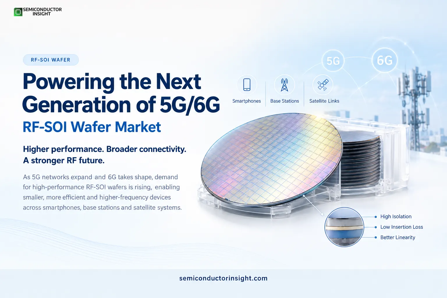
Top RF SOI Wafer Manufacturers Powering 5G Handsets and RF Front-End Modules
The push toward denser 5G and emerging 6G front-end modules continues to elevate demand for specialized RF SOI substrates that deliver superior isolation, lower insertion loss, and better linearity in switches, LNAs, and antenna tuners.
Across smartphone RF chains, base-station designs, and satellite links, these engineered wafers have become the preferred platform for handling multi-band signals without the parasitic effects common in bulk silicon. Here is a closer look at the companies driving production, capacity ramps, and technology advances right now.
Soitec
RF-SOI substrates from this French specialist sit inside virtually every 5G smartphone sold worldwide, with content per device roughly double that of a 4G handset. At the end of fiscal 2025-2026 the Pasir Ris plant in Singapore reached roughly 800,000 300 mm wafers per year of capacity and is already qualified for both RF-SOI and FD-SOI. Bernin 2 in France holds about 750,000 wafers of 300 mm SOI capacity while Bernin 1 contributes up to 750,000 of 200 mm SOI; combined 200 mm and 300 mm lines, together with the Simgui partnership, push total SOI potential well past 2 million wafers annually when fully loaded.
In 2026 the company continued deliberate undershipment of RF-SOI to help customers burn through inventories estimated earlier at 2.5 million 200 mm-equivalent units, while reallocating under-utilized clean-room space toward photonics-SOI and POI lines that share the same manufacturing footprint. Multi-year capacity-reservation agreements with photonics customers and ongoing 300 mm RF-SOI process improvements (including better trap-rich layers and higher-resistivity handles) keep the technology roadmap aligned with sub-8 GHz and FR3 requirements.
Shin-Etsu
High-resistivity SOI wafers from the Japanese materials leader remain a critical second-source option for foundries building RF front-end modules and for emerging optoelectronic-integration programs aimed at lower-power data-center interconnects. The company stably supplies these substrates for next-generation applications that combine optical signal processing with RF circuitry, leveraging its broader silicon-wafer expertise to maintain tight control of oxygen content and resistivity uniformity.
In the current cycle, Shin-Etsu’s SOI output supports customers seeking alternatives for 5G switches and LNAs while also feeding early silicon-photonics development that requires the same low-loss buried-oxide platforms. Continuous refinement of crystal-growth and bonding processes allows the firm to meet the harmonic-performance targets demanded by multi-band smartphone designs without relying solely on external specialty suppliers.
SUMCO
Bonded SOI wafers produced by this Japanese manufacturer serve high-integration RF circuits that need complete electrical isolation and reduced power consumption. The company’s process sandwiches a high-quality oxide layer between polished wafers, enabling devices that combine RF switches with denser digital blocks on the same die.
SUMCO’s SOI line supports both conventional RF front-end needs and more advanced applications where arsenic or antimony diffusion layers are added to the active silicon for optimized device performance. In 2026 the firm continued to position these substrates for customers requiring consistent supply of engineered material that can handle the linearity and isolation demands of sub-6 GHz and millimeter-wave modules.
GlobalWafers
The Taiwanese producer’s Missouri facility stands as the only 12-inch SOI R&D and manufacturing site in the United States, with selected RF and silicon-photonics products entering mass production in the first quarter of 2026. Trial production of 300 mm SOI began earlier and has already delivered positive gross margin on the new line, backed by strong order visibility from customers focused on high-frequency and low-loss applications.
Additional capacity expansions at the Utsunomiya plant in Japan and the Texas fab are progressing through qualification, giving GlobalWafers multiple geographic sources for RF-SOI and related engineered wafers. The company’s independent SOI technology platform allows full in-house control from crystal growth through bonding, supporting both traditional RF switch substrates and newer silicon-photonics designs required for AI data-center optics.
For additional report info, feel free to view our most recent edition: https://semiconductorinsight.com/report/rf-soi-wafer-market/
NSIG (Okmetic)
Volume production at the expanded Vantaa fab in Finland began in early 2026, more than doubling the site’s long-term capacity target by 2030 and significantly increasing 200 mm polished and bonded SOI output for RF, MEMS, and power devices. The expansion adds more than 40,000 m² of space, including a 6,000 m² cleanroom, and builds on earlier investments that doubled bonded SOI capacity between 2017 and 2021.
First wafers from the new lines were produced in June 2025; by February 2026 the company was already shipping from the expanded capacity to customers needing stable European supply of 150–200 mm RF-optimized substrates. High-resistivity RFSi® wafers and cavity-SOI variants continue to serve RF MEMS and front-end applications that require precise membrane control and low parasitic capacitance.
IceMos Technology
Thin-SOI wafers with device layers thinner than 1 µm are produced specifically for RF filters, RF MEMS, wireless connectivity, and silicon-photonics applications. Drawing on more than two decades of SOI bonding experience, the UK-based specialist offers both thick-film and thin-film platforms on 100–200 mm diameters, with thermally grown buried oxides tailored to customer resistivity and thickness targets.
The same process control that supports thick SOI for power and sensor devices is applied to the thinner layers needed for SAW filters and high-frequency RF switches, giving designers a single qualified source for multiple RF-related stacks. Rapid turnaround and Lean Six Sigma process discipline keep the material competitive for prototype-to-volume transitions in 5G front-end and optoelectronic modules.
Wafer Works Corporation
Proprietary bonding and thinning technology developed in-house allows this Taiwanese supplier to deliver customized SOI wafers for RF devices, MEMS, power semiconductors, and silicon photonics. The SOI product family includes B-SOI, multi-layer SOI, cavity SOI, and S-SOI variants optimized for device-layer uniformity and flatness required by analog and RF circuits.
Ultra-high-resistivity polished wafers ready for GaN epitaxy further expand the RF portfolio, while the new Erlin plant’s first 300 mm crystal ingot was pulled in April 2026, positioning additional capacity for future RF-SOI growth. Independent development of the bonding process gives the company control over cost, lead time, and quality for customers seeking alternatives to larger global suppliers.
Shenyang Silicon Technology
Specialized thin-film and thick-film SOI production lines deliver more than 200,000 pieces per year of 6–8 inch material, including ultrathin-film SOI, epitaxial SOI, patterned SOI, and direct-bonded wafers used in RF sensors, MEMS, and optical-communication devices. The company holds proprietary low-temperature microwave annealing thin-film transfer technology and operates more than 90 advanced production and test tools.
These substrates support high-end RF components and gyroscope-level MEMS that require tight thickness control and low defect densities, supplying both domestic Chinese foundries and export customers with cost-effective RF-capable SOI.
Zhonghuan Advanced
Large-scale polished and epitaxial wafer capacity across multiple Chinese sites underpins the firm’s ability to supply base material that can be further processed into RF-SOI stacks. Planned monthly capacities reach 2,100 k slices for 300 mm, 1,400 k slices for 200 mm, and 700 k slices for ≤150 mm wafers, giving ample feedstock for engineered-substrate partners.
The Xuzhou fab focuses on 12-inch IC-grade material certified by international customers, while coordinated sites in Yixing, Tianjin, and Hohhot provide a full range of resistivity and orientation options suitable for high-frequency RF device starting wafers. Continuous improvement in defect-free crystal rates supports the uniformity demands of subsequent SOI bonding steps.
Download your free sample copy of the updated market report: https://semiconductorinsight.com/download-sample-report/?product_id=118052
Shanghai Advanced Silicon Technology
As part of the growing Chinese SOI ecosystem, this producer contributes to domestic supply of engineered substrates used in RF, power, and silicon-photonics applications. Recent progress across the broader Chinese supply chain has brought RF-SOI and related 300 mm products into mass production in 2026, with dedicated capacity supporting BCD, RF, and photonics qualifications.
Local availability of these wafers reduces lead times for Chinese foundries building front-end modules and helps complete a more self-reliant chain from substrate to finished RF die. Capacity expansion plans already target volumes exceeding one million pieces per year to match rising domestic demand for high-isolation RF platforms.

Comments (0)