RF SOI Wafer Market, Trends, Business Strategies 2026-2034

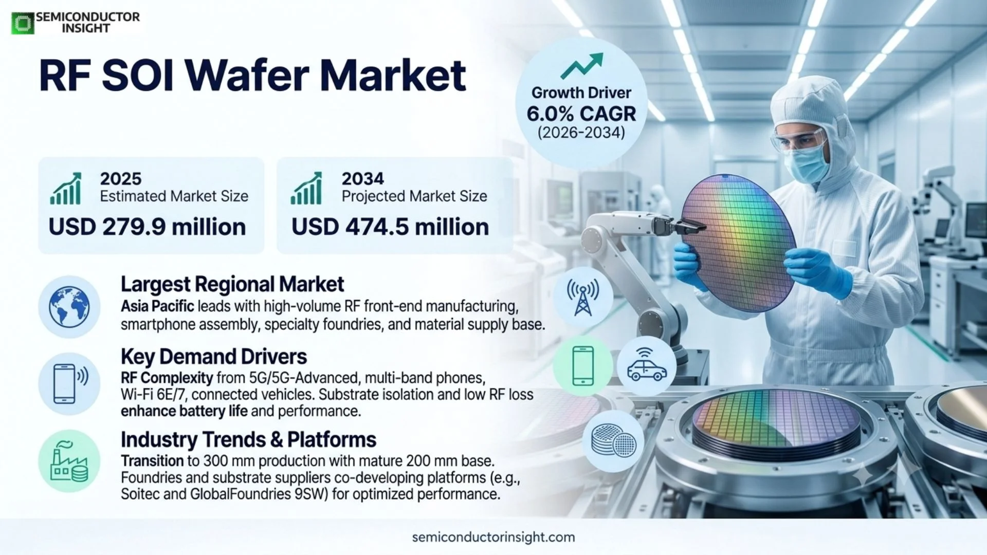
RF SOI Wafer Market is projected to reach USD 474.5 million by 2034, reflecting a 6.0% CAGR during 2026–2034. Asia Pacific is the largest regional market because it combines high-volume RF front-end manufacturing, smartphone assembly, specialty foundries and a large semiconductor-materials supply base.

PDF Icon Download Sample Report PDF
  • Quick Dispatch

    All Orders

  • Secure Payment

    100% Secure Payment

Price range: $1,500.00 through $4,250.00

Clear

Key Statistics

2025 Market Size
USD 279.9 million
2034 Projected Size
USD 474.5 million
CAGR (2026–2034)
6.0%
Largest Market in 2025
Asia Pacific

Key Takeaways

  • 200 mm remains the commercial center of gravity, supported by mature RF-SOI manufacturing equipment, established switch and tuner processes and extensive customer qualification. A quantified product-mix statement places 200 mm at a 58% share, consistent with its installed production base and long qualification history across high-volume RF front-end platforms.
  • 300 mm is the fastest-moving diameter opportunity because newer foundry platforms seek larger-wafer economics and closer alignment with advanced packaging. The shift takes time because RF performance, defectivity and uniformity must be requalified, but each successful 300 mm program raises the technical barrier for suppliers and expands the value of long-term material partnerships.
  • Mobile communications is the largest application because smartphones and connectivity equipment use RF-SOI extensively in switching and tuning. Vehicle electronics is a smaller but attractive diversification route as telematics, navigation, V2X and wireless cabin functions increase, and long automotive qualification cycles can support stable substrate demand after design-in.
  • Asia Pacific leads regional demand through the combination of semiconductor materials, foundry capacity, RF component manufacturing and consumer-electronics assembly in China, Japan, Taiwan and South Korea. North America remains highly influential in RF platform design and foundry technology, while Europe contributes engineered-substrate capability and automotive demand.
  • Inventory correction is the main near-term restraint. Soitec’s fiscal 2025 reporting described weak RF-SOI conditions as customers worked through elevated inventories. This matters because upstream wafer purchases can fall even when end-device demand stabilizes, producing sharper revenue cycles for substrate manufacturers than the underlying smartphone shipment trend would suggest.
  • Competition is qualification-led rather than price-only. Customers require stable resistivity, oxide integrity, thickness uniformity and low defectivity across many lots. Once a wafer is qualified inside a foundry process, changing sources can require re-characterization and yield learning, giving technically proven incumbents a durable advantage and making co-development a major route to share gains.

RF SOI Wafer Market Overview

RF SOI wafer market was valued at USD 279.9 million in 2025 and is projected to reach USD 474.5 million by 2034, reflecting a 6.0% CAGR during 2026–2034. Asia Pacific is the largest regional market because it combines high-volume RF front-end manufacturing, smartphone assembly, specialty foundries and a large semiconductor-materials supply base.

Base year: 2025 · Estimated year: 2026 · Forecast period: 2026–2034 · Historical data: 2021–2025 · Values in USD million

Radio-frequency silicon-on-insulator wafers are engineered substrates used to reduce parasitic capacitance and improve isolation in switches, antenna tuners, low-noise functions and other RF front-end devices. High-resistivity handle wafers, buried oxide and controlled top-silicon thickness help device makers achieve low insertion loss and strong linearity. Wafer quality therefore influences downstream yield, harmonics, power efficiency and the size of compact radio modules.

Demand is tied to radio-frequency complexity rather than simply semiconductor unit volume. Multi-band smartphones, 5G and 5G-Advanced radios, Wi-Fi 6E and Wi-Fi 7 equipment, connected vehicles and specialty communications add signal paths that require switching, filtering and antenna tuning. This raises the value of substrate isolation and consistency because small improvements in RF loss can support better battery life, range and form-factor performance.

The market is gradually adding 300 mm production alongside a mature 200 mm base. Larger wafers can improve fab economics when foundries maintain electrical uniformity and device yield across the expanded area. Soitec and GlobalFoundries have publicly aligned 300 mm RF-SOI with the 9SW platform, showing that substrate suppliers and foundries are increasingly coordinating material, process and packaging roadmaps rather than treating the wafer as a standardized input.

Segment Analysis: By Type

By wafer diameter, the market is segmented into 150 mm and below, 200 mm, and 300 mm. A quantified product-mix statement identifies 200 mm as the dominant format, while 300 mm adoption is accelerating as foundries evaluate larger-wafer economics. The commercial picture is therefore a mature 200 mm volume base with a strategically important transition toward 300 mm manufacturing.

Wafer diameter Manufacturing role Market position
150 mm and Below Smaller-diameter RF-SOI supports legacy specialty processes, development lines and lower-volume applications where installed equipment and existing device qualifications matter more than maximum cost per die. Customers may retain these wafers for mature products because migrating a proven RF device to another diameter can add engineering cost without delivering a meaningful system-performance benefit. The segment has a durable installed base but a weaker structural growth outlook than 200 mm and 300 mm. Its commercial value is concentrated in replacement demand, specialty radio devices and customers with long-lived process flows. Suppliers compete through continuity of supply and preservation of electrical characteristics rather than through a rapid technology-node migration story.
200 mm The 200 mm format is the established workhorse for RF-SOI, aligning with a broad installed base of specialty semiconductor equipment, mature switch and tuner processes, and extensive customer qualifications. The diameter balances manufacturing economics with proven radio-frequency behavior and is deeply embedded in smartphone front-end supply chains that have been optimized over multiple product generations. Largest diameter segment. A quantified product-mix statement places 200 mm at a 58% share and its leadership is consistent with mature manufacturing infrastructure. Even as 300 mm expands, 200 mm remains resilient because front-end products are cost sensitive and qualification intensive, and many high-volume device families already achieve attractive yields on installed 200 mm production lines.
300 mm Larger-diameter wafers can improve fab utilization and yield more die per wafer when paired with compatible high-volume tools. RF-SOI adds the challenge of maintaining substrate uniformity and electrical characteristics across the larger surface. The format is increasingly connected with newer 5G, Wi-Fi and advanced integration roadmaps rather than only with conventional mature-node manufacturing. Fastest-growing diameter opportunity. Soitec and GlobalFoundries have linked 300 mm RF-SOI substrates to the 9SW platform, providing a commercial validation point. Growth depends on qualification and process conversion rather than wafer-area economics alone, but each new program broadens the range of high-volume RF functions that can migrate to 300 mm manufacturing.

How wafer diameter changes supplier economics

Wafer diameter changes die count, asset utilization, handling, metrology and the cost of maintaining uniform electrical properties across the substrate. A supplier that can deliver 300 mm material with repeatable RF characteristics gains access to newer foundry programs, while 200 mm suppliers benefit from a large installed and often depreciated equipment base. The transition therefore depends on qualified total process economics rather than on wafer size alone.

Segment Analysis: By Application

By application, demand is segmented into mobile communications, vehicle electronics and other applications. Mobile communications is the largest use because RF-SOI is deeply embedded in switches and tuners. Vehicle electronics is a smaller but strategically attractive segment because connected vehicles add radio interfaces while automotive programs require long reliability validation, long product lifecycles and dependable supply support.

Application Demand characteristics
Mobile Communications The largest application is driven by smartphones, cellular infrastructure, Wi-Fi devices and other connected products that require low-loss switching and antenna-tuning functions. 5G and 5G-Advanced increase band combinations and RF path complexity, while Wi-Fi 6E and Wi-Fi 7 add high-frequency connectivity. These conditions reward substrate isolation, linearity and consistency when multiple radios operate inside a compact battery-powered device.
Vehicle Electronics Automotive demand comes from telematics, satellite navigation, cellular connectivity, V2X and in-cabin wireless links. The purchasing trigger is the need to maintain performance across temperature, lifetime and reliability requirements rather than raw radio count alone. Once an RF-SOI device is qualified into a vehicle platform, long program duration can support stable material demand and reduce rapid supplier switching.
Others Other demand includes defense communications, industrial wireless equipment, IoT gateways, fixed wireless access and specialty radio systems. Volumes are lower than smartphones, but performance requirements can be demanding and price sensitivity may be lower where RF integrity is mission critical. These applications give suppliers diversification when handset inventories weaken, although qualification and export-control requirements can lengthen sales cycles.

Segmentation by Wafer Material

By wafer material, the market is further divided into high-resistivity and low-resistivity silicon. High-resistivity substrates are central where low RF loss, isolation and linearity matter most, while lower-resistivity material can serve less demanding architectures. Material choice therefore affects both device behavior and the selling-price premium a supplier can defend through tighter electrical specifications and qualification performance.

Wafer material Commercial role
High-Resistivity Silicon Used where low loss, isolation and linearity are critical. These substrates require tight control of resistivity, interfaces and parasitic conduction, increasing the value of materials expertise and statistical process control. The segment benefits most from advanced cellular, Wi-Fi and antenna-tuning designs where substrate behavior can affect battery life, signal integrity and module footprint.
Low-Resistivity Silicon Serves cost-sensitive or technically less demanding designs where conventional silicon characteristics can be accepted within the device architecture. The opportunity is more exposed to price competition because differentiation from substrate electrical performance is narrower. Suppliers depend more heavily on yield consistency, diameter availability and process compatibility than on a large performance-driven material premium.

Segmentation by Fabrication Technology

Fabrication technology is segmented into Smart Cut, bonded SOI and SIMOX. The choice determines how the thin device layer and buried oxide are formed, influencing thickness control, defectivity and manufacturing economics. Smart Cut is important for repeatable commercial layer transfer, while bonded and implanted approaches remain relevant where installed process ownership or specialized material stacks support continued use.

Technology Market implication
Smart Cut Technology Layer-transfer technology supports precise silicon thickness control and scalable SOI manufacturing. Its commercial importance comes from reproducibility across high wafer volumes and compatibility with engineered-substrate roadmaps. Stable material specifications reduce downstream process tuning and improve the chance that an RF device design can be transferred across production lots without losing yield or radio-frequency performance.
Bonded SOI Technology Wafer bonding provides flexibility in combining layers and can support specialized engineered substrates. Its market role depends on bonding quality, interface control and customer-specific stack requirements. The commercial barrier is the need to control voids and thickness uniformity, making supplier experience and metrology capability as important as the nominal bonding method itself.
SIMOX Technology Separation by implanted oxygen forms a buried oxide through implantation and thermal processing. The approach is established but competes with layer-transfer techniques that can provide attractive manufacturing flexibility. SIMOX remains relevant where qualified process flows exist, yet newer RF-SOI programs increasingly emphasize engineered substrate properties and larger-diameter economics associated with modern layer-transfer platforms.

RF SOI Wafer Market Size

Regional Analysis

Asia Pacific is the largest RF SOI wafer market and has the strongest volume-growth foundation because the region concentrates smartphone manufacturing, RF component assembly, specialty foundries and much of the silicon-wafer supply base. North America is strategically important for foundry platforms and wireless design, while Europe remains influential through engineered substrates, automotive electronics and specialty semiconductor capabilities.

Why does RF SOI wafer demand behave differently across regions?

Regional demand follows the location of RF device fabrication, handset and module supply chains, foundry platform ownership and end-market qualification. Asia Pacific converts electronics scale into wafer consumption, North America shapes platform roadmaps, Europe links specialty materials with automotive applications, South America is mainly an imported end-market pull region, and Middle East & Africa is driven more by network deployment than by local substrate manufacturing.

Region Position Growth outlook Demand profile What decides supplier selection
Asia Pacific Largest Highest volume growth Manufacturing-led Scale, local qualification, diameter availability and supply assurance.
North America High strategic influence Steady to strong Foundry and design-led Platform qualification, advanced packaging and secure supply.
Europe Established specialty region Moderate Materials and automotive-led Engineered-substrate performance and long qualification records.
South America Smaller Moderate from low base Import and telecom-led Landed cost and availability of RF components in end systems.
Middle East & Africa Smaller Selective high growth Network-deployment led Telecom projects, equipment availability and global module sourcing.
Asia Pacific LARGEST & FASTEST-GROWING

Why does Asia Pacific lead RF SOI wafer demand?

Asia Pacific leads because the region combines the world’s densest smartphone and RF component supply chains with major foundries and silicon-wafer producers. China provides large handset and telecom demand, Japan contributes advanced materials and wafer technology, Taiwan supplies foundry and RF-device capacity, and South Korea adds mobile ecosystems. This creates both high substrate consumption and strong pressure for local sourcing and second-source qualification.

Market positionLargest region
Growth outlookHighest volume growth
Demand profileManufacturing-led
Market access gateFoundry qualification and local supply assurance
Country Position in region What drives demand
China Largest end-demand pool China combines smartphone production, telecom infrastructure and a developing domestic semiconductor materials base. RF-SOI demand is reinforced by local sourcing initiatives, but qualification standards remain demanding because switch and tuner performance depends on substrate resistivity and defect control. Domestic wafer makers gain share only when they match the statistical consistency required by high-volume RF device processes.
Japan Technology and materials hub Japan is important through silicon-wafer expertise, specialty materials and RF component manufacturing. Suppliers such as Shin-Etsu, SUMCO and SEIREN KST operate within an ecosystem known for disciplined process control. Japanese customers value long qualification records and continuity of supply, supporting premium positions for materials that demonstrate stable electrical performance across multiple product generations.
Taiwan & South Korea Foundry and electronics centers Taiwan links wafer demand to foundry capacity and RF component manufacturing, while South Korea contributes a large mobile and semiconductor ecosystem. The opportunity is strongest for suppliers that support rapid qualification, multiple diameters and reliable logistics. New 300 mm programs are relevant because these markets already operate advanced large-diameter semiconductor infrastructure.

Market instances and commercial signals

The region’s scale advantage comes from clustering handset assembly, RF front-end manufacturing and specialty foundry capacity. This reduces logistics time and lets substrate suppliers work closely with process engineers during qualification. It also raises competitive intensity because customers can compare global and regional sources within the same ecosystem, forcing suppliers to differentiate through yield stability and electrical consistency rather than proximity alone.
China’s localization agenda creates a second-source opportunity for domestic engineered-wafer companies. The barrier remains technical: customers will not trade insertion-loss, linearity or yield performance for local content. Vendors that demonstrate high-resistivity uniformity and stable SOI interfaces can convert strategic interest into commercial qualification, while weaker suppliers remain limited to lower-value or less demanding applications.
Japan and Taiwan are critical to advanced RF-SOI platforms because they combine wafer and foundry-process competence. As devices move toward tighter integration and larger diameters, substrate vendors need sophisticated metrology and customer engineering. The region therefore provides both the largest immediate revenue pool and one of the most demanding environments for new supplier qualification.

Full-report coverage: The complete RF SOI Wafer Market study provides country-level sizing, segment splits, supplier positioning and forecast detail beyond this overview.

North America TECHNOLOGY PLATFORM HUB

Why is North America strategically important despite lower wafer volume?

North America is strategically important because RF architecture, fabless design and specialty-foundry technology can determine substrate requirements used globally. GlobalFoundries’ RF-SOI roadmap and packaging qualification show how foundry decisions in the region create demand for specific diameters and electrical characteristics. Defense communications, premium connectivity and a large semiconductor design ecosystem also support high-value applications where performance and supply assurance matter more than the lowest wafer price.

Market positionHigh strategic influence
Growth outlookSteady to strong
Demand profileFoundry and design-led
Market access gatePlatform qualification, secure supply and technical support
Country Position in region What drives demand
United States Core technology market The United States hosts RF semiconductor design, specialty foundry capability and large communications and defense markets. GlobalFoundries’ 9SW and SLATE work makes the country important for 300 mm RF-SOI evolution. Substrate vendors gain access by qualifying into foundry process flows and demonstrating supply resilience suitable for long-lived commercial and defense programs.
Canada Specialty design and telecom market Canada contributes wireless research, telecom equipment demand and semiconductor design activity rather than large RF-SOI wafer production. Its commercial pull is indirect, flowing through device and module companies that source from global foundries. Suppliers compete on performance documentation, traceability and the ability to support designs manufactured elsewhere but qualified to North American requirements.
Mexico Electronics manufacturing link Mexico’s role is primarily downstream through electronics and automotive manufacturing integrated with North American supply chains. RF-SOI wafer demand is not generated by large local substrate fabs, but connected-vehicle and communications equipment production influences module sourcing. This creates indirect demand for qualified RF components and favors suppliers already embedded in United States and Asian foundry ecosystems.

Market instances and commercial signals

GlobalFoundries’ 9SW roadmap connects substrate selection to a foundry platform used for mobile and 5G radio-frequency applications. When a substrate is qualified at platform level, it can be designed into multiple customer products. That gives wafer suppliers leverage far beyond an isolated spot order and rewards early engineering engagement with the foundry.
The 2026 qualification of SLATE advanced packaging on 9SW reinforces North America’s role in system-level RF integration. The development links wafer properties, device fabrication and three-dimensional packaging, so substrate suppliers must increasingly understand downstream package and thermal requirements. Commercial differentiation moves beyond wafer polish toward co-engineering, process data and confidence that material can support integrated RF architectures.
Defense and aerospace communications provide a smaller but technically demanding demand layer. These programs value traceability, reliability and secure supply and often use longer product lifecycles than consumer handsets. For qualified suppliers, that can stabilize revenue when smartphone inventory cycles weaken, although export controls and program-specific qualification raise market-entry cost.

Full-report coverage: The complete RF SOI Wafer Market study provides country-level sizing, segment splits, supplier positioning and forecast detail beyond this overview.

Europe ENGINEERED MATERIALS & AUTO

What gives Europe a durable role in RF SOI wafers?

Europe combines engineered-substrate leadership with automotive, industrial and specialty semiconductor demand. Soitec’s role makes the region influential upstream even when much downstream fabrication occurs elsewhere. European vehicle platforms also provide a route for RF-SOI through telematics and connectivity. The region therefore competes on materials technology, reliability and long qualification cycles rather than on the highest volume of smartphone assembly.

Market positionEstablished specialty region
Growth outlookModerate
Demand profileMaterials and automotive-led
Market access gateQuality systems, automotive qualification and technology partnerships
Country Position in region What drives demand
France Engineered-substrate center France is strategically important because Soitec is a leading engineered-substrate supplier with extensive RF-SOI expertise and production experience. Its collaborations with global foundries give French substrate technology influence beyond domestic semiconductor volumes. Market access depends on materials performance, long-term co-development and the ability to support 300 mm programs without disrupting mature 200 mm supply.
Germany Automotive demand center Germany contributes through automotive electronics, industrial connectivity and demanding reliability standards. RF-SOI adoption is pulled by telematics, wireless infotainment and connected-vehicle architectures rather than by a large domestic handset industry. Suppliers benefit when downstream RF devices are qualified by European Tier 1s, but the long validation process makes traceability and lifecycle support essential.
United Kingdom & Finland Specialty wafer ecosystem The United Kingdom and Finland contribute specialized wafer and semiconductor capabilities, including IceMos Technology and Okmetic-related operations. These markets show how smaller suppliers can compete through custom specifications and specialty applications. Their opportunity is strongest where global wafer companies are less flexible, provided they maintain RF-grade surface and electrical specifications across production lots.

Market instances and commercial signals

Soitec’s December 2024 collaboration with GlobalFoundries demonstrates Europe’s influence through substrate technology rather than local end-device volume. A French engineered-wafer supplier can shape a platform manufactured and consumed globally when its material becomes part of a foundry reference flow. This export-oriented model supports premium value capture and makes process intellectual property more important than local smartphone assembly.
European automotive customers create a different demand profile from mobile communications. Programs are lower volume but remain in production longer and require extensive reliability validation. Once an RF component based on a specific SOI substrate is qualified into a vehicle platform, suppliers can benefit from sustained demand and lower annual redesign risk, counterbalancing faster consumer-electronics inventory cycles.
Europe’s challenge is cost competitiveness against high-scale Asian manufacturing. Suppliers need to justify higher operating costs through differentiated substrate performance, technical service and secure supply. Investments that improve 300 mm productivity or automate metrology can protect margins, while commodity-oriented products are more vulnerable to price competition from larger wafer producers.

Full-report coverage: The complete RF SOI Wafer Market study provides country-level sizing, segment splits, supplier positioning and forecast detail beyond this overview.

South America IMPORT-DEPENDENT END MARKET

How does South America participate in RF SOI wafers?

South America participates mainly through imported RF components used in telecom infrastructure, smartphones, automotive electronics and connected devices. Brazil is the largest electronics and wireless market in the region, but local RF-SOI wafer fabrication is limited, so demand is transmitted through Asian, North American and European component suppliers. Growth therefore depends on network investment and device replacement rather than domestic engineered-wafer capacity.

Market positionSmaller region
Growth outlookModerate from low base
Demand profileImport and telecom-led
Market access gateLanded cost, distribution and component availability
Country Position in region What drives demand
Brazil Largest regional end market Brazil’s large mobile subscriber base, telecom infrastructure and electronics assembly create the strongest indirect pull for RF-SOI-based components in South America. Wafer suppliers do not usually sell into a local RF foundry; demand is embodied in imported switches, tuners and connectivity modules. Currency movements and import costs therefore influence the region more than local wafer-capacity decisions.
Argentina Selective connectivity market Argentina contributes through mobile networks, enterprise connectivity, automotive imports and consumer electronics. Volumes are smaller than Brazil and exposed to macroeconomic conditions and import availability. RF-SOI demand appears mainly through finished RF modules, so substrate companies capture the opportunity indirectly through global component customers rather than local wafer sales.
Chile Premium connectivity niche Chile supports advanced mobile services, enterprise connectivity and premium devices at a smaller scale. The country’s RF-SOI exposure comes from imported phones, networking equipment and vehicle electronics. Suppliers with broad global customer portfolios capture demand through existing foundry qualifications, while regional channel conditions determine how quickly advanced RF content reaches end users.

Market instances and commercial signals

Regional network modernization increases RF content in devices and infrastructure, but the substrate value is captured upstream outside South America. A wafer may be sold in Asia, fabricated into a switch elsewhere and arrive in Brazil inside a smartphone. End-market tracking is therefore important because direct wafer sales understate the region’s ultimate consumption.
Currency volatility can amplify demand cycles because imported electronics become more expensive when local currencies weaken. That affects smartphone replacement and telecom equipment purchases, which then feeds backward into RF front-end orders. Suppliers cannot manage this through local wafer pricing alone; diversified customers and flexible inventory policies are more effective risk controls.
Automotive connectivity provides gradual diversification as vehicles add telematics, positioning and wireless functions. RF components are generally sourced through global Tier 1 supply chains. Substrate companies benefit when their devices are already qualified in platforms deployed across multiple regions, allowing South American vehicle demand to add incremental volume without a separate material qualification.

Full-report coverage: The complete RF SOI Wafer Market study provides country-level sizing, segment splits, supplier positioning and forecast detail beyond this overview.

Middle East & Africa NETWORK-DEPLOYMENT LED

What drives RF SOI-related demand in Middle East & Africa?

Middle East & Africa is driven mainly by telecom network build-out, premium smartphones, fixed wireless access and connected infrastructure rather than local RF-SOI wafer manufacturing. Gulf markets adopt advanced mobile standards rapidly, while African markets add connectivity through 4G, 5G and fixed wireless. RF-SOI demand is imported inside devices and network modules, making project timing and equipment availability the main regional variables.

Market positionSmaller base
Growth outlookSelective high growth
Demand profileTelecom infrastructure-led
Market access gateNetwork projects, importer channels and equipment-vendor qualification
Country Position in region What drives demand
Gulf Cooperation Council markets High-value connectivity demand Gulf economies invest heavily in advanced mobile networks, smart-city systems and premium connected devices. Their RF-SOI exposure comes through imported smartphones, base-station equipment and fixed wireless access rather than domestic wafer fabs. Suppliers benefit indirectly when global RF component customers win these projects, and premium performance matters where operators prioritize network quality.
South Africa Regional technology hub South Africa has a comparatively developed telecom and enterprise-technology market and acts as a distribution center for parts of sub-Saharan Africa. RF-SOI content arrives through network equipment and consumer devices, so demand follows operator investment and device affordability. The market rewards component suppliers with broad distribution and reliable availability rather than creating a direct substrate sourcing relationship.
UAE & Saudi Arabia Advanced network adopters The UAE and Saudi Arabia deploy advanced cellular networks and smart-infrastructure projects that use increasingly complex RF systems. Their demand profile favors premium connectivity equipment and devices carrying higher RF content. Wafer value is captured upstream through global foundries and module vendors, so substrate companies need strong relationships with those suppliers rather than standalone local sales channels.

Market instances and commercial signals

Advanced mobile-network deployment in Gulf countries increases demand for high-frequency radio components and premium handsets, both of which can use RF-SOI switches and tuners. The commercial path remains indirect because wafers are fabricated elsewhere. Suppliers should therefore monitor telecom equipment and smartphone platform adoption rather than expecting regional substrate orders to mirror end-market growth.
Fixed wireless access is important where fiber deployment is difficult or costly. These systems use sophisticated radio front ends that can benefit from high-isolation switching. Growth in fixed wireless expands the end-use mix beyond smartphones and diversifies substrate demand because infrastructure equipment follows different replacement cycles and inventory dynamics from consumer handsets.
The region remains exposed to project-based volatility. Large telecom or smart-city programs can lift equipment demand quickly, while procurement delays can shift revenue between years. Upstream wafer suppliers should treat this as portfolio demand rather than dedicated capacity justification, using global qualified production to serve project wins without building local substrate assets.

Full-report coverage: The complete RF SOI Wafer Market study provides country-level sizing, segment splits, supplier positioning and forecast detail beyond this overview.

Competitive Landscape

Competition in RF SOI wafers is concentrated around suppliers that combine engineered-substrate capability with high-volume qualification. Customers evaluate resistivity uniformity, defectivity, oxide integrity, thickness control, diameter roadmap and supply continuity rather than nominal wafer specifications alone. This favors companies with deep materials intellectual property, stable manufacturing systems and direct technical relationships with foundries through multi-year process qualifications.

Soitec is strategically important because engineered SOI platforms are embedded in RF front-end supply chains and the company works directly with foundries on newer 300 mm programs. Shin-Etsu, SUMCO and GlobalWafers bring broad wafer-manufacturing scale and customer relationships, while regional suppliers in China, Japan, South Korea, Finland, the United Kingdom and the United States compete through specialty capability and local availability.

Foundry qualification creates a strong retention mechanism. Once a substrate is characterized inside a switch, tuner or front-end process, changing the material can require electrical re-characterization, reliability work and yield re-optimization. Share gains are therefore slower than in standardized commodity materials, but successful qualifications can deliver a long revenue tail, making one platform win more important than short-term spot-price movement.

Price remains relevant in mature 200 mm smartphone programs, but cost must be viewed through device yield and RF performance. A lower-priced substrate that raises defectivity or degrades linearity can be more expensive at module level. Suppliers increasingly compete on total process value, including statistical consistency, technical support, multi-site resilience and a credible roadmap for the 200 mm-to-300 mm transition.

Competitive tier Representative participants How they compete
Engineered-substrate leader Soitec Competes through engineered-wafer technology, extensive RF-SOI qualification and foundry collaboration. The 300 mm relationship with GlobalFoundries demonstrates a platform approach in which substrate development is coordinated with process and packaging roadmaps, raising switching costs and creating a route into higher-density radio-frequency products.
Global wafer majors Shin-Etsu, SUMCO, GlobalWafers Leverage crystal-growth expertise, wafer finishing, global customer access and scale. Their advantage is strongest where customers value multi-site supply, disciplined quality systems and multiple diameters. RF-SOI requires engineered-substrate capability beyond standard polished wafers, so partnerships and specialized process knowledge determine how fully scale converts into share.
Regional specialists NSIG (Okmetic), IceMos, Wafer Works, Chinese suppliers, WaferPro, SEIREN KST, PlutoSemi Compete through proximity, specialty engineering and targeted customer programs. Chinese suppliers benefit from localization priorities, while smaller firms can serve custom specifications overlooked by global majors. Their growth depends on converting sample capability into repeatable volume qualification without compromising resistivity uniformity, layer control or defect performance.

Key Participants

Profiled companies: Soitec (France), Shin-Etsu (Japan), SUMCO (Japan), GlobalWafers (Taiwan), NSIG (Okmetic) (Finland), IceMos Technology (UK), Wafer Works Corporation (Taiwan), Shenyang Silicon Technology (China), Zhonghuan Advanced (China), Shanghai Advanced Silicon Technology (China), WaferPro (U.S.), SEIREN KST (Japan), PlutoSemi (South Korea). The profiled list follows the source-page scope. Competitive relevance differs by diameter, material architecture and qualification depth, so supplier comparisons should be made against the exact RF-SOI specification required by the foundry or device program.

Production Capacity Analysis

RF SOI wafer capacity is constrained by more than crystal-growth tonnage. Commercial capacity requires engineered SOI structures with tight electrical uniformity, low defectivity and repeatable buried-oxide and top-silicon characteristics. The usable capacity pool is therefore narrower than the global polished-silicon wafer base, and moving from 200 mm to 300 mm requires additional process equipment, metrology, qualification and yield learning.

Where production capability is concentrated

High-value RF-SOI production is concentrated among established engineered-substrate and silicon-wafer companies in Europe and Asia, while downstream foundry demand spans Asia, Europe and North America. Soitec’s work with GlobalFoundries illustrates a cross-regional chain in which engineered substrates feed a foundry platform serving mobile and connectivity markets globally. This geographic separation makes logistics discipline, inventory positioning and multi-site contingency planning commercially important.

What constrains usable capacity

Usable capacity is limited by crystal quality, bonding or layer-transfer yield, oxide integrity, thickness uniformity, surface finishing and metrology. A line may have nominal wafer output yet still be unable to serve an RF program if electrical or defect distributions fall outside the customer window. Qualification adds another constraint because capacity cannot be redirected instantly among device processes with different material specifications.

Why 300 mm changes the supply equation

The 300 mm transition can improve scale economics but raises the technical bar. Larger wafers require tighter control of bow, warp, layer thickness and electrical uniformity across a greater area. Foundries also expect stable high-volume delivery because a production interruption affects more die per wafer. Suppliers must fund process development before volume is assured, but successful qualification opens access to newer RF platforms.

Market Dynamics

The RF SOI wafer market is pulled in two directions: wireless systems are adding radio-frequency complexity, supporting structural substrate demand, while handset and component inventory cycles can sharply alter near-term wafer purchases. Structural growth and cyclical corrections therefore coexist. Supplier performance depends on technology positioning, platform qualifications and disciplined capacity management through changes in customer inventory and device launch timing.

5G-Advanced, Wi-Fi 7, carrier aggregation and multi-antenna architectures increase the number of RF paths needing switching, tuning and isolation. That expands the technical role of RF-SOI even when smartphone unit growth is modest. At the same time, module vendors continuously integrate functions to reduce footprint, so wafer suppliers must improve material performance to preserve value rather than assume every added band produces proportional wafer-area growth.

The market is also becoming more platform-driven. GlobalFoundries qualified SLATE advanced packaging on the 9SW RF-SOI platform in 2026 and indicated volume production is expected in the second half of 2027. For substrate suppliers, that means future demand is increasingly tied to co-optimized wafer, process and packaging roadmaps rather than standalone wafer procurement, making foundry collaboration a central commercial capability.

Market Drivers

Commercial forces expanding addressable demand
Driver Impact Commercial mechanism
5G, 5G-Advanced and Wi-Fi radio complexity High Each new cellular band, carrier-aggregation combination and high-band Wi-Fi function adds switching and tuning requirements inside space-constrained devices. RF-SOI provides the isolation and linearity needed to manage these paths efficiently. The commercial response is sustained investment in higher-performance RF processes, increasing the strategic value of consistent high-resistivity substrates and creating new qualification opportunities for advanced wafer suppliers.
Migration toward 300 mm platforms High The move to 300 mm creates a route to higher wafer throughput and closer integration with modern specialty foundries. Soitec and GlobalFoundries have aligned 300 mm substrates with 9SW, demonstrating that the format is moving beyond development work. The commercial implication is a new qualification cycle in which suppliers can win multi-year platform positions if they meet larger-wafer uniformity and defect requirements.
Connected-vehicle RF content Medium Vehicles increasingly combine cellular telematics, GNSS, Wi-Fi, Bluetooth and other wireless links while demanding long reliability lifetimes. RF-SOI devices can support compact, low-loss switching and tuning. Automotive design cycles are slower than handset cycles, but successful qualification produces durable demand, broadening the market beyond consumer electronics and reducing dependence on one annual smartphone replacement cycle.
Advanced packaging and RF integration Medium RF front-end makers seek smaller modules, lower power and better thermal behavior without sacrificing isolation. Foundry-level packaging such as SLATE on RF-SOI platforms creates another route to system shrink. As substrate characteristics become co-optimized with device and package design, material suppliers with deep process partnerships gain a stronger role in platform decisions, supporting premium positioning and longer customer relationships.

5G, 5G-Advanced and Wi-Fi radio complexity

Each new cellular band, carrier-aggregation combination and high-band Wi-Fi function adds switching and tuning requirements inside space-constrained devices. RF-SOI provides the isolation and linearity needed to manage these paths efficiently. The commercial response is sustained investment in higher-performance RF processes, increasing the strategic value of consistent high-resistivity substrates and creating new qualification opportunities for advanced wafer suppliers.

Migration toward 300 mm platforms

The move to 300 mm creates a route to higher wafer throughput and closer integration with modern specialty foundries. Soitec and GlobalFoundries have aligned 300 mm substrates with 9SW, demonstrating that the format is moving beyond development work. The commercial implication is a new qualification cycle in which suppliers can win multi-year platform positions if they meet larger-wafer uniformity and defect requirements.

Connected-vehicle RF content

Vehicles increasingly combine cellular telematics, GNSS, Wi-Fi, Bluetooth and other wireless links while demanding long reliability lifetimes. RF-SOI devices can support compact, low-loss switching and tuning. Automotive design cycles are slower than handset cycles, but successful qualification produces durable demand, broadening the market beyond consumer electronics and reducing dependence on one annual smartphone replacement cycle.

Advanced packaging and RF integration

RF front-end makers seek smaller modules, lower power and better thermal behavior without sacrificing isolation. Foundry-level packaging such as SLATE on RF-SOI platforms creates another route to system shrink. As substrate characteristics become co-optimized with device and package design, material suppliers with deep process partnerships gain a stronger role in platform decisions, supporting premium positioning and longer customer relationships.

Market Restraints

Constraints that limit conversion of end-demand into supplier revenue
Restraint Impact Commercial mechanism
Customer inventory corrections High Upstream wafer demand can contract faster than end-device demand when RF component companies reduce inventory. Soitec reported weak RF-SOI conditions in fiscal 2025 and described elevated customer inventories, showing that the wafer market remains exposed to channel digestion. Suppliers must manage utilization carefully because capacity expanded against temporary orders can become underused when customers normalize stock.
Long qualification cycles Medium An RF-SOI substrate is not freely interchangeable after a device process has been optimized. Changes in resistivity, interface quality, top-silicon thickness or defectivity can affect performance and yield. Customers therefore require extended qualification before approving a new source. This protects incumbents but slows share gains for entrants when the expected savings are small relative to the risk of re-characterizing a mature device.
Smartphone concentration Medium Mobile communications remains the largest end use, leaving the market sensitive to handset production, RF front-end inventory and design changes at a limited number of high-volume customers. Automotive and infrastructure diversify demand, but they cannot immediately absorb a large handset correction. Suppliers need a balanced application portfolio and flexible production planning instead of relying on continuous smartphone content expansion.
Technical difficulty of larger-diameter uniformity Medium The 300 mm opportunity introduces tighter requirements for bow, warp, film thickness, resistivity and defect distribution over a larger surface. A process that works reliably at 200 mm may need meaningful equipment and control-system adaptation. This raises capital and engineering cost and can delay the revenue benefit of announced capacity until statistical process capability and customer qualification are proven.

Customer inventory corrections

Upstream wafer demand can contract faster than end-device demand when RF component companies reduce inventory. Soitec reported weak RF-SOI conditions in fiscal 2025 and described elevated customer inventories, showing that the wafer market remains exposed to channel digestion. Suppliers must manage utilization carefully because capacity expanded against temporary orders can become underused when customers normalize stock.

Long qualification cycles

An RF-SOI substrate is not freely interchangeable after a device process has been optimized. Changes in resistivity, interface quality, top-silicon thickness or defectivity can affect performance and yield. Customers therefore require extended qualification before approving a new source. This protects incumbents but slows share gains for entrants when the expected savings are small relative to the risk of re-characterizing a mature device.

Smartphone concentration

Mobile communications remains the largest end use, leaving the market sensitive to handset production, RF front-end inventory and design changes at a limited number of high-volume customers. Automotive and infrastructure diversify demand, but they cannot immediately absorb a large handset correction. Suppliers need a balanced application portfolio and flexible production planning instead of relying on continuous smartphone content expansion.

Technical difficulty of larger-diameter uniformity

The 300 mm opportunity introduces tighter requirements for bow, warp, film thickness, resistivity and defect distribution over a larger surface. A process that works reliably at 200 mm may need meaningful equipment and control-system adaptation. This raises capital and engineering cost and can delay the revenue benefit of announced capacity until statistical process capability and customer qualification are proven.

Market Opportunities

The strongest opportunities are where RF-SOI solves a system-level bottleneck rather than merely replaces an existing wafer. Higher-frequency connectivity, connected vehicles and advanced packaging make isolation, linearity and footprint more valuable. This favors suppliers that can co-develop substrates with foundries and device makers while supporting both mature 200 mm volume and emerging 300 mm platforms.

300 mm design wins in premium RF front ends

The most attractive near-term opportunity is securing 300 mm qualification in new switch, tuner and integrated front-end processes. Larger-diameter platforms can improve foundry economics and align with advanced packaging. Substrate suppliers that enter early can influence material specifications, creating a stronger competitive position than companies attempting to qualify only after the device architecture and production allocation have already been fixed.

Automotive connectivity platforms

Connected vehicles create a multi-year qualification opportunity across telematics, navigation and V2X connectivity. Automotive customers value long supply continuity and reliability, which can support stable pricing after qualification. Wafer suppliers with strong quality systems and multi-site manufacturing can use these programs to diversify away from handset seasonality and build a revenue stream with longer product lifecycles.

Wi-Fi 7 and converged connectivity modules

Wi-Fi 7 adds bandwidth and radio complexity, increasing the need for efficient switching and coexistence across cellular, Wi-Fi and Bluetooth paths. This creates opportunities in access points, smartphones, PCs and connected consumer products. Suppliers that demonstrate low loss and high linearity at relevant frequencies can capture value even if overall device-unit growth remains moderate.

Regional supply-chain localization

China and other Asian markets are investing in semiconductor supply resilience, creating openings for local wafer suppliers and second-source qualifications. The opportunity is not simple domestic substitution because customers still require RF-grade electrical performance and yield. Suppliers pairing local production with credible process control can gain sourcing share, while established vendors can defend positions through local service and diversified capacity.

Supply Chain Analysis

Silicon & engineered-material inputs
→
RF SOI wafer manufacturing
→
Foundry & RF device fabrication
→
RF modules & end systems

Silicon & engineered-material inputs

The chain begins with high-purity polysilicon, crystal growth and wafer preparation, followed by engineered processes that create the SOI structure. Value is concentrated in resistivity control, bonding or layer transfer, oxide quality and surface finishing. Because RF performance depends on material properties that are difficult to correct later, defects introduced here can destroy downstream value and make qualified suppliers more valuable than lower-priced alternatives.

RF SOI wafer manufacturing

Wafer makers convert base silicon into application-ready engineered substrates, using metrology and statistical control to guarantee thickness, flatness and electrical specifications. This stage captures core substrate value and carries substantial qualification risk. Suppliers must maintain lot-to-lot consistency over years because downstream device makers tune processes to narrow materials windows, particularly in high-volume 200 mm and emerging 300 mm programs.

Foundry & RF device fabrication

Foundries and integrated-device manufacturers fabricate switches, tuners and other RF components on qualified substrates. Their purchasing decision balances wafer price against device yield, RF loss, linearity and process stability. Foundry platforms increasingly integrate RF-SOI with advanced packaging, meaning substrate suppliers that collaborate early can become embedded in reference process flows and gain visibility into future diameter and performance requirements.

RF modules & end systems

RF device makers assemble components into front-end modules sold into smartphones, networking equipment, vehicles and specialty communications. End-system requirements for battery life, antenna performance and compact size flow back into substrate specifications. Inventory corrections also travel backward quickly, so wafer suppliers may see abrupt demand changes when module vendors reduce orders even before end-device shipments move materially.

Recent Developments

Recent developments show RF-SOI moving toward larger-diameter manufacturing and tighter integration with advanced packaging while suppliers remain exposed to cyclical handset inventory. The most important signals are foundry qualification milestones and substrate-platform partnerships that determine which material stacks can enter high-volume radio-frequency production.

23 June 2026

GlobalFoundries qualified SLATE advanced packaging on the 9SW RF-SOI platform

GlobalFoundries announced production readiness for SLATE three-dimensional packaging on 9SW and said volume production is expected in the second half of 2027. The company reports that the approach can reduce die size by up to 45% for certain RF designs, linking RF-SOI with advanced integration and increasing the value of tightly controlled substrates. Source.

27 May 2025

Soitec reported fiscal 2025 RF-SOI inventory pressure alongside design activity

Soitec’s fiscal 2025 results showed weaker mobile-communications revenue and identified RF-SOI customer inventory as a major near-term factor. At the same time, the company highlighted advanced wireless design activity. The combination confirms that structural adoption can continue even while wafer orders are temporarily reduced by inventory digestion, a key planning issue for substrate capacity. Source.

4 December 2024

Soitec and GlobalFoundries expanded collaboration around 300 mm RF-SOI

The companies announced collaboration covering high-performance 300 mm RF-SOI substrates for the 9SW platform. The program targets 5G, 5G-Advanced and Wi-Fi applications and shows that larger-diameter RF-SOI is becoming a commercial foundry roadmap rather than a laboratory option, strengthening the strategic value of suppliers capable of uniform 300 mm engineered substrates. Source.

2023

GlobalFoundries introduced the 9SW RF-SOI technology platform

The 9SW announcement positioned the platform for next-generation mobile and 5G applications with improved RF performance and integration. For wafer suppliers, the platform matters because foundry roadmaps define the electrical and diameter requirements material vendors must meet. The launch also created the foundation for the later 300 mm collaboration and advanced packaging qualification. Source.

Report Scope & Segmentation

Attribute Coverage
Market RF SOI Wafer Market
Base / estimated / forecast years 2025 / 2026 / 2034, with CAGR reported for 2026–2034.
Market size USD 279.9 million in 2025; USD 474.5 million in 2034; 6.0% CAGR for 2026–2034.
By Type 150 mm and Below; 200 mm; 300 mm.
By Application Mobile Communications; Vehicle Electronics; Others.
By Wafer Material High-Resistivity Silicon; Low-Resistivity Silicon.
By Fabrication Technology Smart Cut Technology; Bonded SOI Technology; SIMOX Technology.
Regions North America; Europe; Asia Pacific; South America; Middle East & Africa.
Companies profiled Soitec (France), Shin-Etsu (Japan), SUMCO (Japan), GlobalWafers (Taiwan), NSIG (Okmetic) (Finland), IceMos Technology (UK), Wafer Works Corporation (Taiwan), Shenyang Silicon Technology (China), Zhonghuan Advanced (China), Shanghai Advanced Silicon Technology (China), WaferPro (U.S.), SEIREN KST (Japan), PlutoSemi (South Korea).

Frequently Asked Questions

What is the RF SOI wafer market size in 2025?

The global RF SOI wafer market is valued at USD 279.9 million in 2025. Demand is supported by RF front-end switches, tuners and related connectivity devices that require low-loss, high-isolation substrates. The same 2025 baseline is used consistently across the market overview, forecast, scope and FAQ sections so the article presents one coherent market series.

What is the projected RF SOI wafer market size by 2034?

The market is projected to reach USD 474.5 million by 2034. The projection extends the growth factor implied by the published 2024 and 2032 values, preserving one internally consistent series. Long-term support comes from rising RF complexity in cellular, Wi-Fi, automotive and specialty communications together with gradual migration toward higher-value 300 mm platforms.

What CAGR is expected during 2026–2034?

The market is projected to grow at a 6.0% CAGR during 2026–2034. This rate is mathematically consistent with the 2025 and 2034 market values used throughout the article. Growth is supported by rising RF content per connected device, expanding 5G and Wi-Fi requirements, and gradual 300 mm adoption, while qualification cycles and concentrated engineered-substrate supply moderate the pace of expansion.

Which region is the largest RF SOI wafer market?

Asia Pacific is the largest market in 2025. The region combines smartphone and connectivity-device manufacturing, RF component production, specialty foundry activity and major wafer suppliers across China, Japan, Taiwan and South Korea. This concentration creates high substrate consumption and faster feedback between device changes and wafer qualification while intensifying competition between global suppliers and regional second sources.

Which wafer diameter is the largest segment?

A quantified product-mix statement identifies 200 mm as the dominant diameter, with a 58% share. The format benefits from mature process infrastructure, established switch and tuner flows, and a large installed equipment base. 300 mm is the faster strategic opportunity, but migration requires foundry qualification, larger-wafer uniformity, process portability and customer redesign before large-volume programs can transition.

Why is 300 mm RF SOI important?

300 mm RF SOI can improve manufacturing economics and connect radio-frequency devices to modern large-diameter specialty foundries and advanced packaging. Soitec and GlobalFoundries have collaborated on 300 mm substrates for the 9SW platform. The opportunity is not based on wafer area alone: suppliers must maintain electrical uniformity, defect control and process stability before customers approve volume production.

What is the largest application?

Mobile communications is the largest application, reflecting extensive RF-SOI use in smartphone switches, antenna tuners and connectivity functions. 5G, 5G-Advanced, carrier aggregation and Wi-Fi 7 increase the number and complexity of radio paths managed inside compact devices. This supports substrate value even when handset-unit growth is modest because performance requirements continue to rise.

What is the main restraint on growth?

The most visible near-term restraint is customer inventory correction. Soitec’s fiscal 2025 reporting showed weak RF-SOI conditions associated with elevated inventories, demonstrating that substrate purchases can fall even when end-device demand stabilizes. Long qualification cycles add a second constraint because new suppliers cannot quickly replace incumbents and announced 300 mm capacity may take time to monetize.

Who are the key RF SOI wafer suppliers?

Key profiled suppliers include Soitec, Shin-Etsu, SUMCO, GlobalWafers, NSIG through Okmetic, IceMos Technology, Wafer Works, Shenyang Silicon Technology, Zhonghuan Advanced, Shanghai Advanced Silicon Technology, WaferPro, SEIREN KST and PlutoSemi. Their positions differ by diameter, engineered-substrate capability, manufacturing footprint and qualification depth, so the relevant supplier set varies by foundry platform and end-device program.

How does the RF SOI supply chain create value?

Value is created through high-purity silicon and engineered-material preparation, RF-SOI wafer manufacturing, foundry device fabrication and integration into RF modules and end systems. The most defensible margins sit where errors are costly to correct later. Resistivity, oxide integrity and defectivity affect device yield and RF performance, which is why customers prioritize qualified process consistency and supply assurance over wafer purchase price alone.

Research Sources & Evidence Base

View research sources used for this overview.

  1. GlobalFoundries. RF SOI technology portfolio, technology information covering RF-SOI process families and connectivity applications.
  2. GlobalFoundries. 9SW RF-SOI technology for next-generation mobile and 5G applications, foundry-platform evidence for advanced RF-SOI roadmaps.
  3. GlobalFoundries. SLATE advanced packaging qualified on 9SW, June 2026 production-readiness evidence for RF-SOI advanced packaging.
  4. Soitec. Soitec and GlobalFoundries collaborate on high-performance RF-SOI semiconductors, December 2024 evidence for the 300 mm RF-SOI transition.
  5. Soitec. Fiscal 2025 results, May 2025 evidence on RF-SOI inventory conditions.
  6. Soitec. FY25 results presentation, design-win and customer-inventory context.
RF SOI Wafer Market, Trends, Business Strategies 2026-2034

Get Sample Report PDF for Exclusive Insights

Report Sample Includes

  • Table of Contents
  • List of Tables & Figures
  • Charts, Research Methodology, and more...

PDF Icon Download Sample Report PDF

Download Sample Report

Table of Content

1 Introduction to Research & Analysis Reports
1.1 RF SOI Wafer Market Definition
1.2 Market Segments
1.2.1 Segment by Type
1.2.2 Segment by Application
1.3 Global RF SOI Wafer Market Overview
1.4 Features & Benefits of This Report
1.5 Methodology & Sources of Information
1.5.1 Research Methodology
1.5.2 Research Process
1.5.3 Base Year
1.5.4 Report Assumptions & Caveats
2 Global RF SOI Wafer Overall Market Size
2.1 Global RF SOI Wafer Market Size: 2024 VS 2032
2.2 Global RF SOI Wafer Market Size, Prospects & Forecasts: 2020-2032
2.3 Global RF SOI Wafer Sales: 2020-2032
3 Company Landscape
3.1 Top RF SOI Wafer Players in Global Market
3.2 Top Global RF SOI Wafer Companies Ranked by Revenue
3.3 Global RF SOI Wafer Revenue by Companies
3.4 Global RF SOI Wafer Sales by Companies
3.5 Global RF SOI Wafer Price by Manufacturer (2020-2025)
3.6 Top 3 and Top 5 RF SOI Wafer Companies in Global Market, by Revenue in 2024
3.7 Global Manufacturers RF SOI Wafer Product Type
3.8 Tier 1, Tier 2, and Tier 3 RF SOI Wafer Players in Global Market
3.8.1 List of Global Tier 1 RF SOI Wafer Companies
3.8.2 List of Global Tier 2 and Tier 3 RF SOI Wafer Companies
4 Sights by Product
4.1 Overview
4.1.1 Segment by Type – Global RF SOI Wafer Market Size Markets, 2024 & 2032
4.1.2 150mm and Below
4.1.3 200 mm
4.1.4 300 mm
4.2 Segment by Type – Global RF SOI Wafer Revenue & Forecasts
4.2.1 Segment by Type – Global RF SOI Wafer Revenue, 2020-2025
4.2.2 Segment by Type – Global RF SOI Wafer Revenue, 2026-2032
4.2.3 Segment by Type – Global RF SOI Wafer Revenue Market Share, 2020-2032
4.3 Segment by Type – Global RF SOI Wafer Sales & Forecasts
4.3.1 Segment by Type – Global RF SOI Wafer Sales, 2020-2025
4.3.2 Segment by Type – Global RF SOI Wafer Sales, 2026-2032
4.3.3 Segment by Type – Global RF SOI Wafer Sales Market Share, 2020-2032
4.4 Segment by Type – Global RF SOI Wafer Price (Manufacturers Selling Prices), 2020-2032
5 Sights by Application
5.1 Overview
5.1.1 Segment by Application – Global RF SOI Wafer Market Size, 2024 & 2032
5.1.2 Mobile Communications
5.1.3 Vehicle Electronics
5.1.4 Others
5.2 Segment by Application – Global RF SOI Wafer Revenue & Forecasts
5.2.1 Segment by Application – Global RF SOI Wafer Revenue, 2020-2025
5.2.2 Segment by Application – Global RF SOI Wafer Revenue, 2026-2032
5.2.3 Segment by Application – Global RF SOI Wafer Revenue Market Share, 2020-2032
5.3 Segment by Application – Global RF SOI Wafer Sales & Forecasts
5.3.1 Segment by Application – Global RF SOI Wafer Sales, 2020-2025
5.3.2 Segment by Application – Global RF SOI Wafer Sales, 2026-2032
5.3.3 Segment by Application – Global RF SOI Wafer Sales Market Share, 2020-2032
5.4 Segment by Application – Global RF SOI Wafer Price (Manufacturers Selling Prices), 2020-2032
6 Sights by Region
6.1 By Region – Global RF SOI Wafer Market Size, 2024 & 2032
6.2 By Region – Global RF SOI Wafer Revenue & Forecasts
6.2.1 By Region – Global RF SOI Wafer Revenue, 2020-2025
6.2.2 By Region – Global RF SOI Wafer Revenue, 2026-2032
6.2.3 By Region – Global RF SOI Wafer Revenue Market Share, 2020-2032
6.3 By Region – Global RF SOI Wafer Sales & Forecasts
6.3.1 By Region – Global RF SOI Wafer Sales, 2020-2025
6.3.2 By Region – Global RF SOI Wafer Sales, 2026-2032
6.3.3 By Region – Global RF SOI Wafer Sales Market Share, 2020-2032
6.4 North America
6.4.1 By Country – North America RF SOI Wafer Revenue, 2020-2032
6.4.2 By Country – North America RF SOI Wafer Sales, 2020-2032
6.4.3 United States RF SOI Wafer Market Size, 2020-2032
6.4.4 Canada RF SOI Wafer Market Size, 2020-2032
6.4.5 Mexico RF SOI Wafer Market Size, 2020-2032
6.5 Europe
6.5.1 By Country – Europe RF SOI Wafer Revenue, 2020-2032
6.5.2 By Country – Europe RF SOI Wafer Sales, 2020-2032
6.5.3 Germany RF SOI Wafer Market Size, 2020-2032
6.5.4 France RF SOI Wafer Market Size, 2020-2032
6.5.5 U.K. RF SOI Wafer Market Size, 2020-2032
6.5.6 Italy RF SOI Wafer Market Size, 2020-2032
6.5.7 Russia RF SOI Wafer Market Size, 2020-2032
6.5.8 Nordic Countries RF SOI Wafer Market Size, 2020-2032
6.5.9 Benelux RF SOI Wafer Market Size, 2020-2032
6.6 Asia
6.6.1 By Region – Asia RF SOI Wafer Revenue, 2020-2032
6.6.2 By Region – Asia RF SOI Wafer Sales, 2020-2032
6.6.3 China RF SOI Wafer Market Size, 2020-2032
6.6.4 Japan RF SOI Wafer Market Size, 2020-2032
6.6.5 South Korea RF SOI Wafer Market Size, 2020-2032
6.6.6 Southeast Asia RF SOI Wafer Market Size, 2020-2032
6.6.7 India RF SOI Wafer Market Size, 2020-2032
6.7 South America
6.7.1 By Country – South America RF SOI Wafer Revenue, 2020-2032
6.7.2 By Country – South America RF SOI Wafer Sales, 2020-2032
6.7.3 Brazil RF SOI Wafer Market Size, 2020-2032
6.7.4 Argentina RF SOI Wafer Market Size, 2020-2032
6.8 Middle East & Africa
6.8.1 By Country – Middle East & Africa RF SOI Wafer Revenue, 2020-2032
6.8.2 By Country – Middle East & Africa RF SOI Wafer Sales, 2020-2032
6.8.3 Turkey RF SOI Wafer Market Size, 2020-2032
6.8.4 Israel RF SOI Wafer Market Size, 2020-2032
6.8.5 Saudi Arabia RF SOI Wafer Market Size, 2020-2032
6.8.6 UAE RF SOI Wafer Market Size, 2020-2032
7 Manufacturers & Brands Profiles
7.1 Soitec
7.1.1 Soitec Company Summary
7.1.2 Soitec Business Overview
7.1.3 Soitec RF SOI Wafer Major Product Offerings
7.1.4 Soitec RF SOI Wafer Sales and Revenue in Global (2020-2025)
7.1.5 Soitec Key News & Latest Developments
7.2 Shin-Etsu
7.2.1 Shin-Etsu Company Summary
7.2.2 Shin-Etsu Business Overview
7.2.3 Shin-Etsu RF SOI Wafer Major Product Offerings
7.2.4 Shin-Etsu RF SOI Wafer Sales and Revenue in Global (2020-2025)
7.2.5 Shin-Etsu Key News & Latest Developments
7.3 SUMCO
7.3.1 SUMCO Company Summary
7.3.2 SUMCO Business Overview
7.3.3 SUMCO RF SOI Wafer Major Product Offerings
7.3.4 SUMCO RF SOI Wafer Sales and Revenue in Global (2020-2025)
7.3.5 SUMCO Key News & Latest Developments
7.4 GlobalWafers
7.4.1 GlobalWafers Company Summary
7.4.2 GlobalWafers Business Overview
7.4.3 GlobalWafers RF SOI Wafer Major Product Offerings
7.4.4 GlobalWafers RF SOI Wafer Sales and Revenue in Global (2020-2025)
7.4.5 GlobalWafers Key News & Latest Developments
7.5 NSIG (Okmetic)
7.5.1 NSIG (Okmetic) Company Summary
7.5.2 NSIG (Okmetic) Business Overview
7.5.3 NSIG (Okmetic) RF SOI Wafer Major Product Offerings
7.5.4 NSIG (Okmetic) RF SOI Wafer Sales and Revenue in Global (2020-2025)
7.5.5 NSIG (Okmetic) Key News & Latest Developments
7.6 IceMos Technology
7.6.1 IceMos Technology Company Summary
7.6.2 IceMos Technology Business Overview
7.6.3 IceMos Technology RF SOI Wafer Major Product Offerings
7.6.4 IceMos Technology RF SOI Wafer Sales and Revenue in Global (2020-2025)
7.6.5 IceMos Technology Key News & Latest Developments
7.7 Wafer Works Corporation
7.7.1 Wafer Works Corporation Company Summary
7.7.2 Wafer Works Corporation Business Overview
7.7.3 Wafer Works Corporation RF SOI Wafer Major Product Offerings
7.7.4 Wafer Works Corporation RF SOI Wafer Sales and Revenue in Global (2020-2025)
7.7.5 Wafer Works Corporation Key News & Latest Developments
7.8 Shenyang Silicon Technology
7.8.1 Shenyang Silicon Technology Company Summary
7.8.2 Shenyang Silicon Technology Business Overview
7.8.3 Shenyang Silicon Technology RF SOI Wafer Major Product Offerings
7.8.4 Shenyang Silicon Technology RF SOI Wafer Sales and Revenue in Global (2020-2025)
7.8.5 Shenyang Silicon Technology Key News & Latest Developments
7.9 Zhonghuan Advanced
7.9.1 Zhonghuan Advanced Company Summary
7.9.2 Zhonghuan Advanced Business Overview
7.9.3 Zhonghuan Advanced RF SOI Wafer Major Product Offerings
7.9.4 Zhonghuan Advanced RF SOI Wafer Sales and Revenue in Global (2020-2025)
7.9.5 Zhonghuan Advanced Key News & Latest Developments
7.10 Shanghai Advanced Silicon Technology
7.10.1 Shanghai Advanced Silicon Technology Company Summary
7.10.2 Shanghai Advanced Silicon Technology Business Overview
7.10.3 Shanghai Advanced Silicon Technology RF SOI Wafer Major Product Offerings
7.10.4 Shanghai Advanced Silicon Technology RF SOI Wafer Sales and Revenue in Global (2020-2025)
7.10.5 Shanghai Advanced Silicon Technology Key News & Latest Developments
7.11 WaferPro
7.11.1 WaferPro Company Summary
7.11.2 WaferPro Business Overview
7.11.3 WaferPro RF SOI Wafer Major Product Offerings
7.11.4 WaferPro RF SOI Wafer Sales and Revenue in Global (2020-2025)
7.11.5 WaferPro Key News & Latest Developments
7.12 SEIREN KST
7.12.1 SEIREN KST Company Summary
7.12.2 SEIREN KST Business Overview
7.12.3 SEIREN KST RF SOI Wafer Major Product Offerings
7.12.4 SEIREN KST RF SOI Wafer Sales and Revenue in Global (2020-2025)
7.12.5 SEIREN KST Key News & Latest Developments
7.13 PlutoSemi
7.13.1 PlutoSemi Company Summary
7.13.2 PlutoSemi Business Overview
7.13.3 PlutoSemi RF SOI Wafer Major Product Offerings
7.13.4 PlutoSemi RF SOI Wafer Sales and Revenue in Global (2020-2025)
7.13.5 PlutoSemi Key News & Latest Developments
8 Global RF SOI Wafer Production Capacity, Analysis
8.1 Global RF SOI Wafer Production Capacity, 2020-2032
8.2 RF SOI Wafer Production Capacity of Key Manufacturers in Global Market
8.3 Global RF SOI Wafer Production by Region
9 Key Market Trends, Opportunity, Drivers and Restraints
9.1 Market Opportunities & Trends
9.2 Market Drivers
9.3 Market Restraints
10 RF SOI Wafer Supply Chain Analysis
10.1 RF SOI Wafer Industry Value Chain
10.2 RF SOI Wafer Upstream Market
10.3 RF SOI Wafer Downstream and Clients
10.4 Marketing Channels Analysis
10.4.1 Marketing Channels
10.4.2 RF SOI Wafer Distributors and Sales Agents in Global
11 Conclusion
12 Appendix
12.1 Note
12.2 Examples of Clients
12.3 DisclaimerList of Tables
Table 1. Key Players of RF SOI Wafer in Global Market
Table 2. Top RF SOI Wafer Players in Global Market, Ranking by Revenue (2024)
Table 3. Global RF SOI Wafer Revenue by Companies, (US$, Mn), 2020-2025
Table 4. Global RF SOI Wafer Revenue Share by Companies, 2020-2025
Table 5. Global RF SOI Wafer Sales by Companies, (K Pcs), 2020-2025
Table 6. Global RF SOI Wafer Sales Share by Companies, 2020-2025
Table 7. Key Manufacturers RF SOI Wafer Price (2020-2025) & (US$/Pcs)
Table 8. Global Manufacturers RF SOI Wafer Product Type
Table 9. List of Global Tier 1 RF SOI Wafer Companies, Revenue (US$, Mn) in 2024 and Market Share
Table 10. List of Global Tier 2 and Tier 3 RF SOI Wafer Companies, Revenue (US$, Mn) in 2024 and Market Share
Table 11. Segment by Type – Global RF SOI Wafer Revenue, (US$, Mn), 2024 & 2032
Table 12. Segment by Type – Global RF SOI Wafer Revenue (US$, Mn), 2020-2025
Table 13. Segment by Type – Global RF SOI Wafer Revenue (US$, Mn), 2026-2032
Table 14. Segment by Type – Global RF SOI Wafer Sales (K Pcs), 2020-2025
Table 15. Segment by Type – Global RF SOI Wafer Sales (K Pcs), 2026-2032
Table 16. Segment by Application – Global RF SOI Wafer Revenue, (US$, Mn), 2024 & 2032
Table 17. Segment by Application – Global RF SOI Wafer Revenue, (US$, Mn), 2020-2025
Table 18. Segment by Application – Global RF SOI Wafer Revenue, (US$, Mn), 2026-2032
Table 19. Segment by Application – Global RF SOI Wafer Sales, (K Pcs), 2020-2025
Table 20. Segment by Application – Global RF SOI Wafer Sales, (K Pcs), 2026-2032
Table 21. By Region – Global RF SOI Wafer Revenue, (US$, Mn), 2025-2032
Table 22. By Region – Global RF SOI Wafer Revenue, (US$, Mn), 2020-2025
Table 23. By Region – Global RF SOI Wafer Revenue, (US$, Mn), 2026-2032
Table 24. By Region – Global RF SOI Wafer Sales, (K Pcs), 2020-2025
Table 25. By Region – Global RF SOI Wafer Sales, (K Pcs), 2026-2032
Table 26. By Country – North America RF SOI Wafer Revenue, (US$, Mn), 2020-2025
Table 27. By Country – North America RF SOI Wafer Revenue, (US$, Mn), 2026-2032
Table 28. By Country – North America RF SOI Wafer Sales, (K Pcs), 2020-2025
Table 29. By Country – North America RF SOI Wafer Sales, (K Pcs), 2026-2032
Table 30. By Country – Europe RF SOI Wafer Revenue, (US$, Mn), 2020-2025
Table 31. By Country – Europe RF SOI Wafer Revenue, (US$, Mn), 2026-2032
Table 32. By Country – Europe RF SOI Wafer Sales, (K Pcs), 2020-2025
Table 33. By Country – Europe RF SOI Wafer Sales, (K Pcs), 2026-2032
Table 34. By Region – Asia RF SOI Wafer Revenue, (US$, Mn), 2020-2025
Table 35. By Region – Asia RF SOI Wafer Revenue, (US$, Mn), 2026-2032
Table 36. By Region – Asia RF SOI Wafer Sales, (K Pcs), 2020-2025
Table 37. By Region – Asia RF SOI Wafer Sales, (K Pcs), 2026-2032
Table 38. By Country – South America RF SOI Wafer Revenue, (US$, Mn), 2020-2025
Table 39. By Country – South America RF SOI Wafer Revenue, (US$, Mn), 2026-2032
Table 40. By Country – South America RF SOI Wafer Sales, (K Pcs), 2020-2025
Table 41. By Country – South America RF SOI Wafer Sales, (K Pcs), 2026-2032
Table 42. By Country – Middle East & Africa RF SOI Wafer Revenue, (US$, Mn), 2020-2025
Table 43. By Country – Middle East & Africa RF SOI Wafer Revenue, (US$, Mn), 2026-2032
Table 44. By Country – Middle East & Africa RF SOI Wafer Sales, (K Pcs), 2020-2025
Table 45. By Country – Middle East & Africa RF SOI Wafer Sales, (K Pcs), 2026-2032
Table 46. Soitec Company Summary
Table 47. Soitec RF SOI Wafer Product Offerings
Table 48. Soitec RF SOI Wafer Sales (K Pcs), Revenue (US$, Mn) and Average Price (US$/Pcs) & (2020-2025)
Table 49. Soitec Key News & Latest Developments
Table 50. Shin-Etsu Company Summary
Table 51. Shin-Etsu RF SOI Wafer Product Offerings
Table 52. Shin-Etsu RF SOI Wafer Sales (K Pcs), Revenue (US$, Mn) and Average Price (US$/Pcs) & (2020-2025)
Table 53. Shin-Etsu Key News & Latest Developments
Table 54. SUMCO Company Summary
Table 55. SUMCO RF SOI Wafer Product Offerings
Table 56. SUMCO RF SOI Wafer Sales (K Pcs), Revenue (US$, Mn) and Average Price (US$/Pcs) & (2020-2025)
Table 57. SUMCO Key News & Latest Developments
Table 58. GlobalWafers Company Summary
Table 59. GlobalWafers RF SOI Wafer Product Offerings
Table 60. GlobalWafers RF SOI Wafer Sales (K Pcs), Revenue (US$, Mn) and Average Price (US$/Pcs) & (2020-2025)
Table 61. GlobalWafers Key News & Latest Developments
Table 62. NSIG (Okmetic) Company Summary
Table 63. NSIG (Okmetic) RF SOI Wafer Product Offerings
Table 64. NSIG (Okmetic) RF SOI Wafer Sales (K Pcs), Revenue (US$, Mn) and Average Price (US$/Pcs) & (2020-2025)
Table 65. NSIG (Okmetic) Key News & Latest Developments
Table 66. IceMos Technology Company Summary
Table 67. IceMos Technology RF SOI Wafer Product Offerings
Table 68. IceMos Technology RF SOI Wafer Sales (K Pcs), Revenue (US$, Mn) and Average Price (US$/Pcs) & (2020-2025)
Table 69. IceMos Technology Key News & Latest Developments
Table 70. Wafer Works Corporation Company Summary
Table 71. Wafer Works Corporation RF SOI Wafer Product Offerings
Table 72. Wafer Works Corporation RF SOI Wafer Sales (K Pcs), Revenue (US$, Mn) and Average Price (US$/Pcs) & (2020-2025)
Table 73. Wafer Works Corporation Key News & Latest Developments
Table 74. Shenyang Silicon Technology Company Summary
Table 75. Shenyang Silicon Technology RF SOI Wafer Product Offerings
Table 76. Shenyang Silicon Technology RF SOI Wafer Sales (K Pcs), Revenue (US$, Mn) and Average Price (US$/Pcs) & (2020-2025)
Table 77. Shenyang Silicon Technology Key News & Latest Developments
Table 78. Zhonghuan Advanced Company Summary
Table 79. Zhonghuan Advanced RF SOI Wafer Product Offerings
Table 80. Zhonghuan Advanced RF SOI Wafer Sales (K Pcs), Revenue (US$, Mn) and Average Price (US$/Pcs) & (2020-2025)
Table 81. Zhonghuan Advanced Key News & Latest Developments
Table 82. Shanghai Advanced Silicon Technology Company Summary
Table 83. Shanghai Advanced Silicon Technology RF SOI Wafer Product Offerings
Table 84. Shanghai Advanced Silicon Technology RF SOI Wafer Sales (K Pcs), Revenue (US$, Mn) and Average Price (US$/Pcs) & (2020-2025)
Table 85. Shanghai Advanced Silicon Technology Key News & Latest Developments
Table 86. WaferPro Company Summary
Table 87. WaferPro RF SOI Wafer Product Offerings
Table 88. WaferPro RF SOI Wafer Sales (K Pcs), Revenue (US$, Mn) and Average Price (US$/Pcs) & (2020-2025)
Table 89. WaferPro Key News & Latest Developments
Table 90. SEIREN KST Company Summary
Table 91. SEIREN KST RF SOI Wafer Product Offerings
Table 92. SEIREN KST RF SOI Wafer Sales (K Pcs), Revenue (US$, Mn) and Average Price (US$/Pcs) & (2020-2025)
Table 93. SEIREN KST Key News & Latest Developments
Table 94. PlutoSemi Company Summary
Table 95. PlutoSemi RF SOI Wafer Product Offerings
Table 96. PlutoSemi RF SOI Wafer Sales (K Pcs), Revenue (US$, Mn) and Average Price (US$/Pcs) & (2020-2025)
Table 97. PlutoSemi Key News & Latest Developments
Table 98. RF SOI Wafer Capacity of Key Manufacturers in Global Market, 2023-2025 (K Pcs)
Table 99. Global RF SOI Wafer Capacity Market Share of Key Manufacturers, 2023-2025
Table 100. Global RF SOI Wafer Production by Region, 2020-2025 (K Pcs)
Table 101. Global RF SOI Wafer Production by Region, 2026-2032 (K Pcs)
Table 102. RF SOI Wafer Market Opportunities & Trends in Global Market
Table 103. RF SOI Wafer Market Drivers in Global Market
Table 104. RF SOI Wafer Market Restraints in Global Market
Table 105. RF SOI Wafer Raw Materials
Table 106. RF SOI Wafer Raw Materials Suppliers in Global Market
Table 107. Typical RF SOI Wafer Downstream
Table 108. RF SOI Wafer Downstream Clients in Global Market
Table 109. RF SOI Wafer Distributors and Sales Agents in Global Market

List of Figures
Figure 1. RF SOI Wafer Product Picture
Figure 2. RF SOI Wafer Segment by Type in 2024
Figure 3. RF SOI Wafer Segment by Application in 2024
Figure 4. Global RF SOI Wafer Market Overview: 2024
Figure 5. Key Caveats
Figure 6. Global RF SOI Wafer Market Size: 2024 VS 2032 (US$, Mn)
Figure 7. Global RF SOI Wafer Revenue: 2020-2032 (US$, Mn)
Figure 8. RF SOI Wafer Sales in Global Market: 2020-2032 (K Pcs)
Figure 9. The Top 3 and 5 Players Market Share by RF SOI Wafer Revenue in 2024
Figure 10. Segment by Type – Global RF SOI Wafer Revenue, (US$, Mn), 2024 & 2032
Figure 11. Segment by Type – Global RF SOI Wafer Revenue Market Share, 2020-2032
Figure 12. Segment by Type – Global RF SOI Wafer Sales Market Share, 2020-2032
Figure 13. Segment by Type – Global RF SOI Wafer Price (US$/Pcs), 2020-2032
Figure 14. Segment by Application – Global RF SOI Wafer Revenue, (US$, Mn), 2024 & 2032
Figure 15. Segment by Application – Global RF SOI Wafer Revenue Market Share, 2020-2032
Figure 16. Segment by Application – Global RF SOI Wafer Sales Market Share, 2020-2032
Figure 17. Segment by Application -Global RF SOI Wafer Price (US$/Pcs), 2020-2032
Figure 18. By Region – Global RF SOI Wafer Revenue, (US$, Mn), 2025 & 2032
Figure 19. By Region – Global RF SOI Wafer Revenue Market Share, 2020 VS 2024 VS 2032
Figure 20. By Region – Global RF SOI Wafer Revenue Market Share, 2020-2032
Figure 21. By Region – Global RF SOI Wafer Sales Market Share, 2020-2032
Figure 22. By Country – North America RF SOI Wafer Revenue Market Share, 2020-2032
Figure 23. By Country – North America RF SOI Wafer Sales Market Share, 2020-2032
Figure 24. United States RF SOI Wafer Revenue, (US$, Mn), 2020-2032
Figure 25. Canada RF SOI Wafer Revenue, (US$, Mn), 2020-2032
Figure 26. Mexico RF SOI Wafer Revenue, (US$, Mn), 2020-2032
Figure 27. By Country – Europe RF SOI Wafer Revenue Market Share, 2020-2032
Figure 28. By Country – Europe RF SOI Wafer Sales Market Share, 2020-2032
Figure 29. Germany RF SOI Wafer Revenue, (US$, Mn), 2020-2032
Figure 30. France RF SOI Wafer Revenue, (US$, Mn), 2020-2032
Figure 31. U.K. RF SOI Wafer Revenue, (US$, Mn), 2020-2032
Figure 32. Italy RF SOI Wafer Revenue, (US$, Mn), 2020-2032
Figure 33. Russia RF SOI Wafer Revenue, (US$, Mn), 2020-2032
Figure 34. Nordic Countries RF SOI Wafer Revenue, (US$, Mn), 2020-2032
Figure 35. Benelux RF SOI Wafer Revenue, (US$, Mn), 2020-2032
Figure 36. By Region – Asia RF SOI Wafer Revenue Market Share, 2020-2032
Figure 37. By Region – Asia RF SOI Wafer Sales Market Share, 2020-2032
Figure 38. China RF SOI Wafer Revenue, (US$, Mn), 2020-2032
Figure 39. Japan RF SOI Wafer Revenue, (US$, Mn), 2020-2032
Figure 40. South Korea RF SOI Wafer Revenue, (US$, Mn), 2020-2032
Figure 41. Southeast Asia RF SOI Wafer Revenue, (US$, Mn), 2020-2032
Figure 42. India RF SOI Wafer Revenue, (US$, Mn), 2020-2032
Figure 43. By Country – South America RF SOI Wafer Revenue Market Share, 2020-2032
Figure 44. By Country – South America RF SOI Wafer Sales, Market Share, 2020-2032
Figure 45. Brazil RF SOI Wafer Revenue, (US$, Mn), 2020-2032
Figure 46. Argentina RF SOI Wafer Revenue, (US$, Mn), 2020-2032
Figure 47. By Country – Middle East & Africa RF SOI Wafer Revenue, Market Share, 2020-2032
Figure 48. By Country – Middle East & Africa RF SOI Wafer Sales, Market Share, 2020-2032
Figure 49. Turkey RF SOI Wafer Revenue, (US$, Mn), 2020-2032
Figure 50. Israel RF SOI Wafer Revenue, (US$, Mn), 2020-2032
Figure 51. Saudi Arabia RF SOI Wafer Revenue, (US$, Mn), 2020-2032
Figure 52. UAE RF SOI Wafer Revenue, (US$, Mn), 2020-2032
Figure 53. Global RF SOI Wafer Production Capacity (K Pcs), 2020-2032
Figure 54. The Percentage of Production RF SOI Wafer by Region, 2024 VS 2032
Figure 55. RF SOI Wafer Industry Value Chain
Figure 56. Marketing Channels