
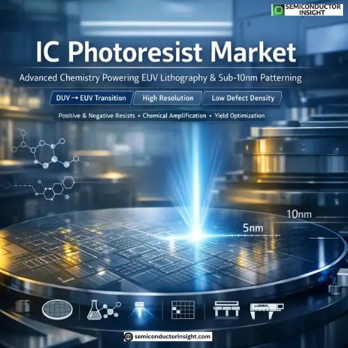
The Strategic Role of IC Photoresists Market in Semiconductor Manufacturing Precision
In semiconductor fabrication, a wafer is a blank canvas and light is the brush. But what allows that light to draw the intricate pathways of transistors and interconnects? IC photoresists specialized chemical formulations that respond to illumination are the enablers of this transformation. They translate optical or extreme ultraviolet (EUV) energy into physical patterns on silicon surfaces, defining the circuits that power modern electronics.
Photoresists are not passive coatings; they are chemically engineered polymers that undergo targeted reactions when exposed to specific wavelengths. These reactions produce solubility changes that allow selective removal, enabling nanometre-scale pattern transfer. In effect, the advancement of a semiconductor node can often be traced back to the capability of its photoresist chemistry.
Before Proceeding, Feel Free to Overlook Our Updated Report:
https://semiconductorinsight.com/report/global-ic-photoresist-market/
The Role of Photoresists in Semiconductor Lithography
Lithography is the heart of patterning in semiconductor manufacturing, and photoresists are its core consumable. A typical lithography cycle involves coating a wafer with photoresist, exposing it to controlled radiation, developing the exposed pattern, etching, and then stripping the resist.
Two broad categories dominate:
- Positive photoresists, where exposed areas become soluble
- Negative photoresists, where exposed areas become cross-linked and insoluble
At advanced nodes particularly sub-10 nm and EUV patterning photoresists must deliver high resolution, low line edge roughness, and excellent etch resistance. This requires fine-tuned polymer backbones, sensitizers, and additives carefully balanced for performance, manufacturability, and defect control.
Material Science Driving Photoresist Innovation
IC photoresists are complex blends of polymers, photo-acid generators (PAGs), sensitizers, resins, and solvents. The advancements comes from engineering molecules that react predictably to light yet remain stable under fabrication conditions.
Some of the key chemistry challenges and innovations include:
- Absorption control: Matching resist chemistry to EUV wavelengths to maximize sensitivity without compromising resolution
- Chemical amplification: Using PAGs that generate acids on exposure, triggering cascade reactions for efficient solubility shifts
- Low outgassing formulations: Essential for EUV to minimize contamination of optical elements
- Etch resistance tuning: Balancing organic and inorganic content to withstand plasma etching
As pattern densities increase and critical dimensions shrink, the photochemical response and mechanical robustness of resists are continuously refined.
Transitioning from DUV to EUV: Market Implications
Historically, deep ultraviolet (DUV) lithography using 193 nm light dominated most production. However, the push toward higher integration and finer geometries has accelerated the adoption of EUV lithography.
EUV systems operate at ~13.5 nm wavelengths, offering superior resolution but placing new demands on photoresist materials:
- Enhanced sensitivity to minimize exposure times
- Minimized stochastic defects that can hamper yield
- Tailored acid diffusion lengths for consistent pattern fidelity
These requirements have opened a new tier of materials innovation, leading to dedicated EUV resist platforms from leading chemical suppliers. The market for EUV photoresists, while still emerging relative to DUV demand, is experiencing strong initial adoption in leading-edge fabs.
Yield, Defects, and Productivity The Downstream Significance
In semiconductor manufacturing, yield is king. A single defect at the photoresist patterning stage can propagate through etch, deposition, and metallization, reducing overall wafer yield. As a result, photoresist performance directly correlates with fab productivity metrics.
Manufacturers monitor:
- Line edge roughness (LER) as a proxy for pattern smoothness
- Critical dimension uniformity (CDU) across the wafer
- Resist resolution limits relative to exposure tool capabilities
- Stochastic defect density in high-volume production
Improvements in resist chemistry that reduce defect density even marginally can translate into millions of dollars in recovered output for high-capacity fabs.
Environmental and Regulatory Dimensions
Photoresists and their ancillary chemistries are subject to environmental and safety regulations. Resist components are handled under strict controls for worker safety, waste management, and solvent emissions. Regulatory trends are motivating suppliers to:
- Develop lower-solvent or solvent-free formulations
- Reduce hazardous additive content where possible
- Improve recycling and waste treatment practices
While performance remains paramount, regulatory compliance and sustainability are increasingly shaping product development decisions.
IC photoresist market is a vivid example of how core chemistry underpins technological evolution. From enabling pattern definition at 100 nm nodes to facilitating EUV patterning at sub-10 nm dimensions, photoresists have evolved in lockstep with device innovation.
For semiconductor stakeholders whether material suppliers, foundries, or equipment partners understanding this market means appreciating the interplay between chemical performance, lithography advancement, and yield optimization. In an industry where every nanometer matters, the role of IC photoresists remains fundamental to progress.

Comments (0)