
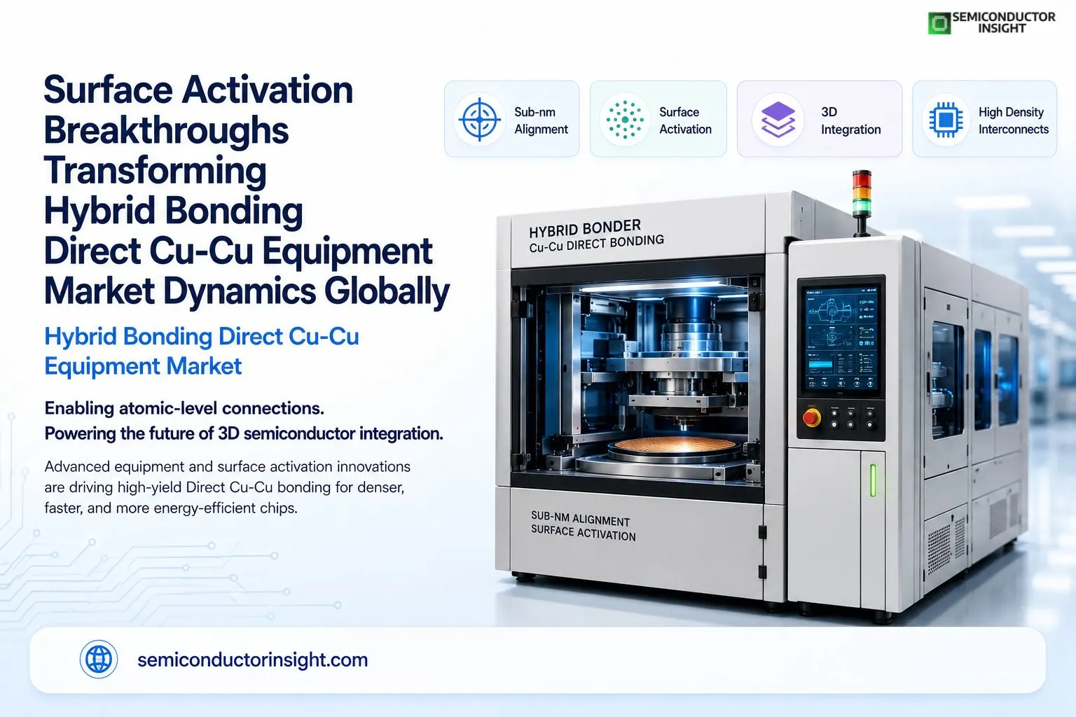
Surface Activation Breakthroughs Transforming Hybrid Bonding Direct Cu-Cu Equipment Market Dynamics Globally
Semiconductor manufacturing continues pushing boundaries as traditional scaling faces physical limits. Hybrid bonding, particularly direct copper-to-copper connections, emerges as a pivotal approach enabling denser, more efficient vertical stacking of chips.
This technology bonds dielectric surfaces while creating simultaneous metal interconnects without relying on solder bumps, allowing for significantly finer pitches and improved performance.
Tracing the Evolution of Direct Bonding Techniques
- Early concepts of copper-to-copper wafer bonding trace back to research at MIT around 1999, where teams explored ways to stack integrated circuits vertically for better performance and smaller footprints.
- Over time, this evolved into hybrid methods combining oxide-to-oxide dielectric bonding with embedded copper pads.
- Entries on three-dimensional integrated circuits highlight how Cu-Cu connections, alongside through-silicon vias, help devices behave as single units while reducing power needs.
- Initial commercial steps appeared in image sensors, where wafer-to-wafer bonding delivered reliable results.
- Sony’s adoption in CMOS image sensors marked an early high-volume success, paving the way for broader exploration in memory and logic applications. These foundations set the stage for today’s equipment focused on achieving atomic-level cleanliness and alignment precision.
Precision Alignment and Surface Preparation Breakthroughs
Achieving successful direct Cu-Cu bonds requires surfaces flat to sub-nanometer levels, with copper pads recessed just enough for reliable contact. Equipment now incorporates advanced chemical-mechanical planarization, plasma activation, and ultra-precise alignment systems capable of handling sub-micron accuracies. Research from institutions like Imec demonstrates pitches reaching 400 nanometers in wafer-to-wafer configurations, showcasing what dedicated bonding tools can accomplish.
Cleanroom standards play a crucial role here. Processes often demand ISO 3 or better environments, sometimes reaching ISO 1 or 2 for high-yield production. This front-end-like requirement influences equipment design, pushing manufacturers toward integrated platforms that combine multiple steps while maintaining contamination control.
Equipment Ecosystem Driving Technical Progress
Tool makers develop specialized bonders, cleaners, and metrology systems tailored for hybrid processes. Platforms handle wafer-to-wafer flows for uniform stacks and die-to-wafer variants for heterogeneous chiplets. Features like multi-chamber architectures support surface activation, alignment, and bonding in controlled sequences to minimize defects.
Applied Materials contributes deposition, CMP, and etch solutions optimized for hybrid flows. Tokyo Electron advances bonding and debonding systems, while partners focus on pick-and-place accuracy for individual dies. These tools address key hurdles like thermal budgets and alignment tolerances essential for production scaling.
Explore the full report details in our recently refreshed edition anytime: https://semiconductorinsight.com/report/hybrid-bonding-direct-cu-cu-equipment-market/
Performance Advantages in High-Compute Applications
- Direct Cu-Cu links deliver bandwidth densities far exceeding older methods, with interconnects potentially reaching millions per square millimeter. This supports AI accelerators and high-performance computing where latency and power efficiency matter critically. Reduced parasitics improve signal integrity, while closer integration enhances thermal dissipation paths.
- In photonics and sensor integrations, hybrid approaches allow mixing different process nodes and materials seamlessly. Government and academic efforts worldwide, including projects on university sites and public research portals, continue refining materials like SiCN dielectrics for stronger, lower-temperature bonds.
Global Collaboration and Supply Chain Maturation
International research consortia and company partnerships speed up standardization. European labs, Asian foundries, and North American innovators share insights on reliability testing and process optimization. Equipment suppliers expand capabilities to support both high-volume memory lines and custom logic configurations.
Case studies from technical conferences reveal ongoing work on pitches below one micron, with demonstrations showing robust mechanical strength and electrical performance after thermal cycling. These examples illustrate how hybrid bonding equipment evolves to meet diverse industry needs, from mobile devices to data center infrastructure.
Emerging Use Cases Expanding Market Reach
- Beyond traditional logic-memory stacks, applications in automotive sensors, edge AI devices, and advanced imaging benefit from compact, power-efficient designs. Co-packaged optics integrations explore hybrid bonding for tighter electrical-optical connections. As chiplet architectures proliferate, equipment enabling flexible die placement gains importance.
- Ongoing magazine features and journal articles detail how surface-activated bonding variants lower temperature requirements, broadening compatibility with sensitive components. These developments keep the technology relevant across expanding semiconductor segments.
The hybrid bonding direct Cu-Cu equipment space reflects deeper industry shifts toward three-dimensional thinking. With continued refinements in tools and processes, it stands ready to support the complex, high-efficiency systems defining tomorrow’s electronics.

Comments (0)