
Semiconductor Copper Wire Bonding Equipment Market Accelerating with Next-Gen Chip Packaging
Copper wire bonding equipment is emerging as a backbone technology in modern semiconductor packaging, replacing traditional gold bonding in many high-volume applications.
As chipmakers push toward cost efficiency and higher electrical performance, copper has become the preferred interconnect material reshaping the equipment landscape that enables this transition.
Shift from Gold to Copper Transforming Equipment Demand
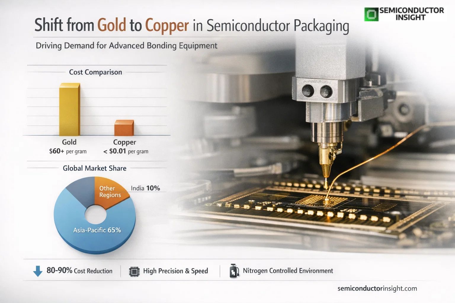
The transition from gold to copper bonding is not just a material swap it represents a structural change in semiconductor manufacturing. Copper is nearly 80-90% cheaper than gold, making it highly attractive for large-scale chip production. While gold prices often exceed $60 per gram, copper remains below $0.01 per gram, drastically reducing packaging costs for devices produced in billions of units annually.
However, copper introduces complexity. It oxidizes easily and requires controlled environments, advanced bonding tools, and precise process parameters. This has led to a surge in demand for high-precision copper wire bonding equipment capable of maintaining reliability under strict conditions.
A Closer Look at Our Latest Study and Key Findings: https://semiconductorinsight.com/report/semiconductor-copper-wire-bonding-equipment-market/
Engineering Complexity Driving Equipment Innovation
- Copper wire bonding equipment is significantly more advanced than its predecessors. These machines integrate real-time monitoring systems, ultrasonic bonding technology, and advanced capillary designs to ensure stable connections at microscopic levels.
- Modern bonders can operate at speeds exceeding 10 wires per second, handling ultra-fine wire diameters as low as 15 microns. The equipment must also maintain consistent bonding force, temperature, and ultrasonic energy, often within extremely tight tolerances.
- To prevent oxidation, many systems now operate in nitrogen-rich environments, adding another layer of engineering sophistication. This complexity has increased the average cost of copper wire bonding machines, often ranging from $120,000 to $500,000 per unit depending on capability and automation level.
Application Expansion across High-Growth Semiconductor Segments
Copper wire bonding equipment is widely used across multiple semiconductor segments, particularly where cost-performance balance is critical.
In consumer electronics, devices like smartphones and wearable’s rely heavily on copper bonding due to their high production volumes. With over 1.2 billion smartphones shipped globally each year, even minor cost reductions per chip translate into significant savings.
In automotive electronics, copper bonding is gaining traction in power devices and control units. Electric vehicles, which can contain over 3,000 semiconductor chips per unit, are driving demand for reliable and thermally stable interconnect solutions.
Industrial electronics and IoT devices are also contributing to market growth, where durability and cost efficiency are equally important.
Types of Copper Wire Bonding Equipment in Modern Fabrication
- The market is segmented based on bonding techniques and levels of automation, each serving distinct manufacturing needs.
- Ball bonding equipment is the most widely used, especially for integrated circuits, due to its speed and adaptability.
- Wedge bonding systems are preferred in power electronics, offering stronger mechanical connections and better performance in high-current applications.
- Fully automated bonding machines dominate large-scale production facilities, integrating AI-based inspection and process optimization tools.
- Manual and semi-automatic systems still find relevance in small-batch production and specialized applications, where flexibility is more important than speed.
- Each type reflects a balance between throughput, precision, and cost, allowing manufacturers to tailor equipment to their production strategies.
Production Scale and Equipment Utilization Insights
Globally, semiconductor packaging facilities operate thousands of wire bonding machines, with leading fabs running over 500 bonding units per facility. Equipment utilization rates are typically high, often exceeding 85% uptime, reflecting the continuous nature of chip production.
Asia-Pacific leads the market, accounting for the majority of installations due to the concentration of semiconductor manufacturing in countries like China, Taiwan, South Korea, and Malaysia.
India is also entering the ecosystem with new semiconductor initiatives, which are expected to increase demand for packaging equipment, including copper wire bonders, in the coming years.
Material Science Advancements Enhancing Bonding Reliability
- Recent innovations in copper wire materials are improving bonding performance and reliability. Palladium-coated copper (PCC) wires are gaining popularity as they reduce oxidation risks and enhance bond strength.
- These wires, combined with advanced bonding equipment, enable longer device lifespans and better resistance to environmental stress. In high-reliability sectors like automotive and aerospace, such advancements are critical.
- Additionally, improvements in capillary materials and bonding algorithms are allowing machines to handle increasingly complex chip designs, supporting the trend toward miniaturization.
Expanding Opportunities Shaped by Cutting Edge Chip Design and AI Enabled Systems
The future of copper wire bonding equipment is closely tied to the evolution of semiconductor packaging. While advanced packaging technologies like 3D stacking and chiplets are gaining attention, copper bonding continues to serve as a cost-effective solution for a vast range of applications.
AI chips, data centers, and edge computing devices are expected to sustain high demand for semiconductor components, indirectly boosting the need for efficient bonding equipment.
As manufacturers strive to balance cost, performance, and scalability, copper wire bonding equipment will remain a critical enabler in the semiconductor value chain, adapting continuously to meet the demands of next-generation electronics.

Comments (0)