
Leading Semiconductor Fabs Expand Capacity Supporting the Wafer Testing Service Market
The semiconductor industry is racing toward smaller process nodes, faster processors, and increasingly complex chip designs. While much of the attention focuses on fabrication technologies and advanced packaging, wafer testing has quietly become one of the most critical stages in semiconductor manufacturing. Before a silicon wafer is separated into individual chips, every die must undergo electrical testing to verify its functionality and identify defects. This early screening helps manufacturers avoid unnecessary packaging costs, improve production efficiency, and maintain high product reliability.
As artificial intelligence, automotive electronics, 5G infrastructure, and high performance computing continue to expand, semiconductor manufacturers are placing greater emphasis on precision testing services. Modern wafer testing providers are no longer limited to detecting defective chips. They now contribute valuable production data that helps improve yield, optimize manufacturing processes, and accelerate the commercialization of advanced semiconductor devices.
Every Functional Chip Starts With a Reliable Wafer Test
- Wafer testing serves as the first electrical checkpoint after the manufacturing process is completed.
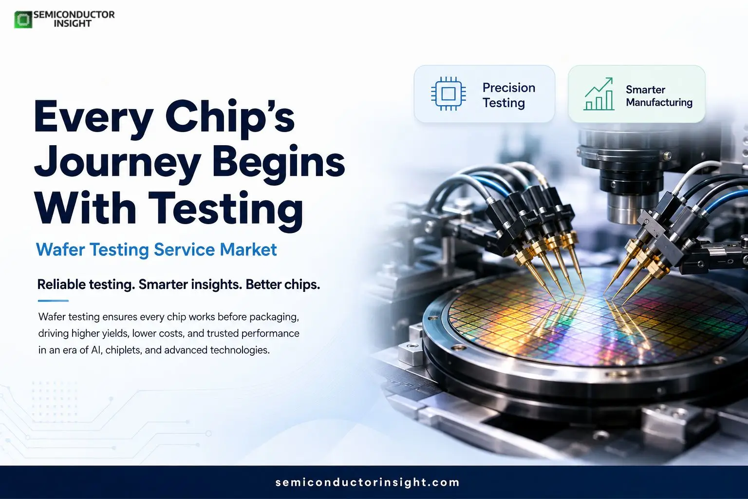
- Using automated probe stations equipped with microscopic probe needles, each integrated circuit on the wafer is evaluated before moving to packaging.
- This process confirms whether a chip performs according to design specifications while identifying defective dies that should be excluded from the production flow.
- The importance of this stage has increased significantly as transistor dimensions continue to shrink.
- Today’s advanced logic chips integrate tens of billions of transistors onto a single die, making even the smallest manufacturing variation capable of affecting device performance. Detecting these issues before packaging saves both time and manufacturing resources while supporting consistent product quality.
- Industries such as consumer electronics, cloud computing, industrial automation, telecommunications, and automotive manufacturing all depend on wafer testing to ensure reliable semiconductor performance before products enter the market.
For More Detailed Insights, You Can Surf Our Latest Report Here: https://semiconductorinsight.com/report/wafer-testing-service-market/
The Scale of Modern Semiconductor Manufacturing Demands Smarter Testing
The complexity of semiconductor production has grown dramatically over the past decade. According to Semiconductor Equipment and Materials International (SEMI), 300 mm wafers have become the industry standard for high-volume manufacturing because they produce significantly more chips per wafer than earlier 200 mm platforms, improving manufacturing efficiency.
Modern semiconductor fabrication also involves several hundred individual processing steps before electrical testing begins. During these stages, wafers undergo oxidation, deposition, photolithography, etching, ion implantation, cleaning, and chemical mechanical polishing. Every process introduces variables that must be verified before chips proceed to packaging.
Extreme Ultraviolet (EUV) lithography systems, developed for manufacturing advanced semiconductor nodes, contain more than 100,000 individual components, according to ASML. The precision required throughout fabrication highlights why equally sophisticated wafer testing has become indispensable for maintaining manufacturing quality.
Artificial Intelligence Is Changing What Wafer Testing Must Deliver
- Artificial intelligence has influenced not only the chips being manufactured but also the way semiconductor testing is performed. AI accelerators, graphics processors, neural processing units, and high bandwidth memory devices require far more comprehensive electrical characterization than previous generations of semiconductors.
- Manufacturers producing AI processors operate under extremely high performance expectations where minor electrical inconsistencies can reduce computational efficiency or increase power consumption. As a result, wafer testing now includes advanced parametric measurements, leakage current analysis, signal integrity verification, and statistical process monitoring that provide engineers with deeper insight into manufacturing performance.
- Leading semiconductor manufacturers continue expanding production capacity for AI hardware. TSMC has significantly increased advanced packaging capacity for AI applications, while Intel Foundry and Samsung Foundry continue investing in next-generation process technologies designed for increasingly sophisticated semiconductor products. These developments are creating sustained demand for specialized wafer testing services capable of handling advanced device architectures.
Chiplet Designs Are Expanding the Scope of Wafer Testing
The semiconductor industry is rapidly adopting chiplet architectures to overcome the physical and economic limitations of traditional monolithic chips. Instead of manufacturing one large processor, multiple specialized chiplets are fabricated separately and later integrated into a single package. This design approach improves flexibility, enhances performance, and allows manufacturers to combine components built on different process technologies.
However, chiplets introduce a new level of testing complexity. Every individual die must be electrically verified before assembly because replacing a faulty chiplet after advanced packaging is both expensive and time consuming. Wafer testing services therefore perform detailed functional verification, interconnect validation, and parametric measurements to ensure each chiplet meets performance requirements before integration.
Recent technologies such as AMD’s chiplet-based EPYC and Ryzen processors, and TSMC’s CoWoS advanced packaging platform demonstrate how advanced integration is increasing the importance of wafer-level testing. As heterogeneous integration becomes more common across AI processors and high performance computing systems, testing services continue expanding their capabilities to support increasingly sophisticated semiconductor designs.
Today’s Wafer Testing Labs Blend Precision Hardware with Intelligent Software
- Modern wafer testing laboratories are highly automated environments where robotics, precision mechanics, advanced electronics, and data analytics operate together. Automated wafer probers position microscopic probe needles with remarkable accuracy, allowing electrical measurements to be performed on every die without damaging delicate semiconductor structures.
- Alongside the hardware, sophisticated software platforms continuously analyze measurement results to identify process variation and optimize production. Statistical process control, automated yield analysis, defect mapping, and machine learning algorithms enable engineers to detect trends that would be difficult to recognize through manual inspection alone.
Some advanced production facilities can generate millions of individual test data points every day, creating valuable manufacturing intelligence that supports process optimization, faster root-cause analysis, and improved production consistency. Rather than simply filtering defective chips, wafer testing has become an important source of operational insight throughout semiconductor manufacturing.

Comments (0)