Wafer Testing Service Market Insights
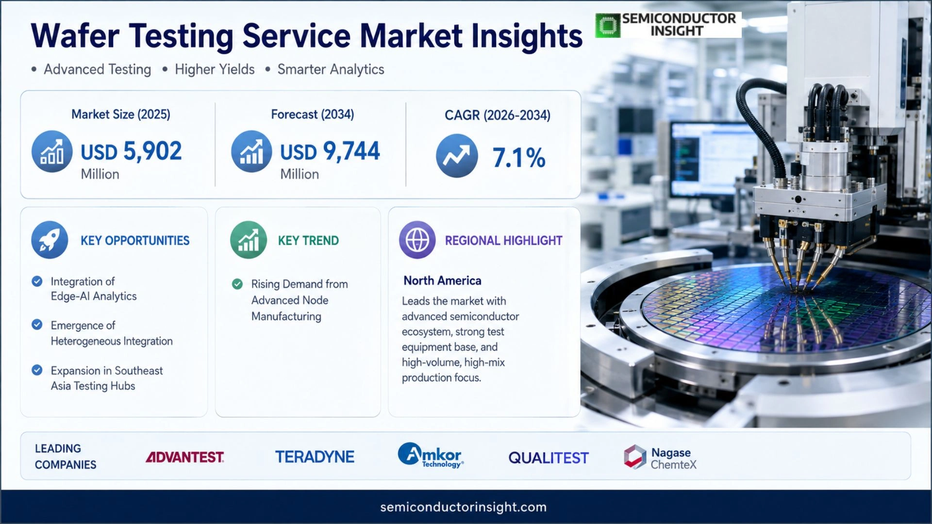
Wafer Testing Service market size was valued at USD 5,902 million in 2025. The market is projected to reach USD 9,744 million by 2034, exhibiting a CAGR of 7.1% during the forecast period.
Wafer Testing Service refers to the professional testing process performed on a fully processed semiconductor wafer before die singulation and packaging. Electrical parameters, functional performance and reliability of each die are examined using probe equipment to screen out defective dies, generate a wafer map and reduce packaging costs while improving final product yield.
Growth is supported by rising downstream semiconductor demand, increasing complexity of advanced nodes such as 5 nm and below, and stricter reliability requirements in automotive and medical applications. However, high equipment investment and supply‑chain volatility pose challenges for service providers.
MARKET DRIVERS
Advanced Semiconductor Architectures
The transition to sub‑10 nm nodes forces manufacturers to verify electrical performance with unprecedented granularity. Precision measurement at the wafer level uncovers defects that would otherwise manifest only after costly die‑level testing, thereby safeguarding yield. Wafer Testing Service Market providers that embed AI‑assisted analysis are gaining preference because they translate raw data into actionable process tweaks.
Regulatory Compliance and Reliability Demands
Automotive and aerospace certifications now mandate traceable test records for each silicon lot. Suppliers that can furnish audit‑ready reports reduce the time‑to‑market for safety‑critical chips. This compliance pressure pushes fab operators toward integrated testing solutions rather than ad‑hoc laboratory checks.
➤ Clients that embed continuous wafer‑level monitoring report up to 12 % higher first‑pass yield compared with batch‑only strategies.
From a financial standpoint, the cost offset derived from early defect detection exceeds the incremental expense of advanced testing platforms, prompting a shift in capital allocation toward scalable wafer‑testing services.
MARKET CHALLENGES
Escalating Test Equipment Costs
State‑of‑the‑art probing stations and high‑resolution metrology tools command multi‑million dollar price tags. Smaller fabs, in particular, struggle to amortize these assets over limited production volumes, leading to a reliance on external service bureaus.
Other Challenges
Skilled Workforce Shortage
The sophistication of modern test algorithms requires engineers fluent in both semiconductor physics and machine‑learning frameworks. Talent pipelines have not kept pace, creating bottlenecks for firms eager to expand service offerings.
MARKET RESTRAINTS
Capital Intensity of Scaling Operations
Expanding wafer‑testing capacity entails not only equipment upgrades but also clean‑room expansions and rigorous validation cycles. The upfront outlay often exceeds the budget thresholds of emerging market participants, limiting competitive entry.
Furthermore, the long lead times for critical components,such as high‑speed data acquisition boards,can delay project timelines, forcing customers to postpone deployment of new test lines.
Lastly, contractual negotiations for service level agreements frequently involve extensive risk‑sharing clauses, which can deter firms from committing to large‑scale outsourcing arrangements.
MARKET OPPORTUNITIES
Integration of Edge‑AI Analytics
Embedding lightweight AI models directly into test equipment enables real‑time defect classification, reducing data transfer latency. Service providers that master this integration can offer differentiated insights, opening premium pricing tiers.
Emergence of Heterogeneous Integration
As chip designers increasingly combine logic, memory, and photonic components on a single wafer, testing protocols must evolve to address cross‑domain interactions. Companies that develop multi‑modal test suites stand to capture a sizable share of the upcoming demand wave.
Finally, the rise of regional semiconductor clusters in Southeast Asia presents a geographic expansion avenue. Localized testing hubs can reduce logistics costs for fabless firms, while also complying with increasingly stringent regional data‑handling regulations.
Wafer Testing Service Market Trends
Rising Demand from Advanced Node Manufacturing
The surge in chip architectures below 5 nm is compelling fab operators to rely heavily on wafer‑level validation. As each die becomes more expensive, customers insist on early detection of electrical anomalies to safeguard final yields. This pressure is magnified by the expanding share of automotive and high‑frequency applications, where a single faulty die can jeopardize safety certifications. Consequently, service providers are expanding capacity for 12‑inch wafers, where testing fees for advanced nodes now top $2,500 per wafer, reflecting the higher instrumentation complexity. The net effect is a tighter coupling between downstream fab output and the testing value chain, prompting OEMs to negotiate longer‑term contracts that embed yield‑share clauses.
Other Trends
Supply‑Chain Volatility and Equipment Investment
Recent disruptions in the procurement of high‑precision probe cards and lithography‑compatible test heads have introduced scheduling uncertainty for test houses. Capital expenditures to upgrade to sub‑3 nm capable platforms exceed $150 million, a hurdle that filters out smaller players and accelerates consolidation. The heightened entry barrier forces mid‑size firms to seek joint ventures or acquire niche equipment vendors to maintain service continuity. From a strategic standpoint, this environment rewards entities with diversified supplier bases and robust after‑sales support networks, as they can sustain throughput despite component shortages.
Customization Pressure versus Delivery Speed
Customers increasingly request bespoke test vectors tailored to emerging architectures such as heterogeneous integration and chip‑let assemblies. While these bespoke solutions improve functional confidence, they extend the test cycle by up to 30 %, straining the tight launch timelines typical of consumer electronics. Service providers are therefore investing in modular automation frameworks that can swap test scripts with minimal downtime. The business implication is a shift toward value‑added pricing models, where the margin derives from engineering expertise rather than pure throughput. Companies that master this balance are positioned to capture higher‑margin contracts, especially in sectors where reliability standards are non‑negotiable.
COMPETITIVE LANDSCAPE
Key Industry Players
Competitive Overview of Wafer Testing Service Providers
The wafer‑testing segment is dominated by a handful of vertically integrated conglomerates that leverage both equipment manufacturing and test execution capabilities. ASE Holdings, with its extensive probe‑card portfolio and global test house network, commands the largest share of outsourced testing contracts, especially for mature‑node and emerging 3D‑IC workloads. TSMC operates an in‑house testing division that supports its fab services, allowing the foundry to offer a seamless flow from wafer fabrication to final qualification, a proposition that appeals to high‑volume customers seeking tight schedule alignment. Samsung’s semiconductor arm also runs a sizable internal test operation, chiefly targeting its own memory and logic lines while occasionally opening capacity to external clients. Their scale enables aggressive amortization of multi‑million‑dollar probe‑card tooling, which in turn squeezes margins for smaller niche operators. Consequently, the competitive landscape revolves around the ability to offer differentiated test methodologies, rapid turn‑around, and robust yield‑improvement analytics.
Beyond the tier‑one houses, a diverse cohort of specialist test providers has carved out profitable niches by focusing on particular process windows or regional markets. KYEC, based in China, has become a go‑to partner for 12‑inch wafer testing in the 28nm‑to‑7nm window, leveraging cost‑effective probe cards and a flexible scheduling model. JCET and its subsidiary Tongfu Microelectronics supply integrated assembly‑and‑test services to fabless firms, emphasizing high‑mix, low‑volume orders that larger players often overlook. Amkor and PTI extend their expertise from package testing into wafer‑level validation, offering bundled solutions that appeal to clients pursuing system‑in‑package designs. Companies such as Wise Road, ChipMOS, and SFA Semiconductor differentiate themselves through advanced reliability testing suites tailored for automotive and medical ICs, where failure‑rate specifications are markedly tighter. The presence of these focused firms injects competitive pressure, prompting the larger houses to broaden service portfolios and refine value‑added analytics.
List of Key Wafer Testing Service Companies Profiled
- ASE Holdings
- KYEC
- TSMC
- Samsung Electronics
- Amkor Technology
- PTI
- JCET Group
- Tongfu Microelectronics
- Wise Road
- ChipMOS Technologies
- SFA Semiconductor
- OSE (Open Semiconductor)
- Intel Corporation
Segment Analysis:
| Segment Category | Sub-Segments | Key Insights |
| By Type |
|
Electrical Parameter Testing is the leading segment because it provides the earliest detection of defects, which helps manufacturers preserve yield and avoid costly downstream rework. – Focuses on precise voltage, current, and resistance measurements that underpin chip functionality. – Aligns tightly with evolving node complexity, ensuring that even the most advanced designs meet stringent quality standards. – Supports cross‑industry reliability expectations, especially in sectors where failure is not an option. |
| By Application |
|
Automotive emerges as the dominant application segment due to the heightened reliability and safety mandates of vehicle electronics. – Requires rigorous testing for temperature extremes and vibration resilience. – Drives demand for comprehensive functional and reliability assessments throughout the wafer stage. – Encourages close collaboration between test houses and OEM supply chains to meet certification timelines. |
| By End User |
|
Fabless Companies lead this segment because they rely heavily on specialist test houses to validate design integrity before tape‑out. – Prioritize flexible testing solutions that adapt quickly to design revisions. – Value the cost efficiencies of outsourcing complex wafer‑level examinations. – Seek partners that can integrate testing data into their overall product development workflow. |
| By Service Provider |
|
Independent Test Houses dominate because they offer neutral, best‑in‑class expertise across multiple fab customers. – Provide scalable capacity that can absorb spikes in demand from diverse design houses. – Maintain a technology‑agnostic approach, staying ahead of node transitions. – Enable manufacturers to benchmark yield performance against industry peers. |
| By Wafer & Process |
|
12‑inch Wafer Testing is the focal point as the industry shifts toward larger diameters for cost efficiencies. – Supports both mature and leading‑edge process nodes, offering flexibility to customers. – Enhances throughput, allowing tighter time‑to‑market schedules. – Aligns with the push for higher integration densities in emerging applications such as AI accelerators. |
Regional Analysis: Wafer Testing Service Market
North America
Silicon Valley, Austin, and the Research Triangle concentrate R&D spend on test‑algorithm development, shortening the feedback loop between design and silicon validation, which accelerates time‑to‑market for new devices.
Close ties between fab operators and test service firms enable just‑in‑time delivery of test modules, cutting inventory costs and allowing rapid scale‑up during demand spikes for high‑performance chips.
Universities such as MIT and Stanford supply a steady stream of engineers versed in mixed‑signal testing, ensuring service providers can staff complex projects without relying on overseas expertise.
Recent policy frameworks emphasize domestic semiconductor resilience, prompting increased funding for test infrastructure that meets stringent security and reliability standards.
Europe
European nations, particularly Germany and the Netherlands, leverage a strong tradition of precision engineering to differentiate their Wafer Testing Service Market participation. OEMs benefit from test providers that embed statistical process control within their workflows, allowing tighter defect budgets for advanced logic and RF devices. Collaboration between EU research programs and industry consortia fosters cross‑border standards that streamline data exchange, reducing the friction of moving wafers between member states. While demand for high‑volume automotive semiconductors dominates, niche markets such as aerospace and medical devices drive bespoke test solutions that prioritize long‑term reliability over sheer throughput. The regulatory environment, guided by GDPR‑aligned data handling, also shapes how companies capture and analyze test metrics, reinforcing a culture of traceability and auditability.
Asia‑Pacific
The Asia‑Pacific region remains a hotbed for wafer fabrication, and its testing services are evolving from cost‑focused offerings to value‑added partnerships. Countries like Taiwan, South Korea, and Singapore invest heavily in AI‑enhanced defect classification, enabling fab operators to pinpoint yield loss with unprecedented granularity. This shift is propelled by the intense competition among foundries to support cutting‑edge nodes, where marginal yield improvements translate directly into profit. Moreover, the rise of smart manufacturing initiatives encourages test providers to embed IoT sensors within tester equipment, feeding real‑time performance data back to production planners. The result is a more dynamic testing ecosystem that can flexibly respond to rapid technology transitions while maintaining strict quality benchmarks.
South America
South America’s contribution to Wafer Testing Service market is anchored by emerging semiconductor assembly hubs in Brazil and Chile. Although the region lacks large‑scale fabs, it has cultivated a niche in intermediate test services for mixed‑signal and power devices destined for automotive and renewable‑energy applications. Local providers differentiate themselves through cost‑effective labor structures combined with tailored support for legacy process nodes, where mature technologies still command significant demand. Government incentives aimed at fostering a domestic semiconductor supply chain have spurred investments in test automation, gradually raising the technical baseline and enabling South American firms to compete for offshore contracts.
Middle East & Africa
The Middle East & Africa segment is gradually entering Wafer Testing Service market, driven primarily by strategic diversification efforts in the United Arab Emirates and Saudi Arabia. These economies are channeling sovereign wealth into semiconductor test labs that serve regional defense and telecommunications projects, emphasizing security‑focused testing protocols. African nations, while still nascent, are exploring partnerships with Asian test firms to upskill local engineers and establish pilot facilities for low‑volume specialty chips. The overarching trend is a cautious but deliberate move toward building indigenous testing capabilities, thereby reducing reliance on distant service hubs and aligning with broader initiatives to develop a self‑sufficient technology ecosystem.
Report Scope
This market research report provides a comprehensive analysis of the Wafer Testing Service Market , covering the forecast period 2026–2034. It offers detailed insights into market dynamics, technological advancements, competitive landscape, and key trends shaping the industry.
Key focus areas of the report include:
- Market Overview: The report begins with an overview outlining its current market scenario, key growth indicators, and industry transformation drivers. It discusses macroeconomic factors, demand–supply balance, regulatory landscape, and the strategic role of semiconductors in powering advancements across industries such as automotive, telecommunications, consumer electronics, and industrial automation.
- Market Size & Forecast: Historical data and future projections for revenue, unit shipments, and market value across major regions and segments.
- Segmentation Analysis: Detailed breakdown by product type, technology, application, and end-user industry to identify high-growth segments and investment opportunities.
- Regional Insights: Insights into market performance across North America, Europe, Asia-Pacific, Latin America, and the Middle East & Africa, including country-level analysis where relevant.
- Competitive Landscape: Profiles of leading market participants, including their product offerings, R&D focus, manufacturing capacity, pricing strategies, and recent developments such as mergers, acquisitions, and partnerships.
- Technology Trends & Innovation: Assessment of emerging technologies, integration of AI/IoT, semiconductor design trends, fabrication techniques, and evolving industry standards.
- Market Drivers & Restraints: Evaluation of factors driving market growth along with challenges, supply chain constraints, regulatory issues, and market-entry barriers.
- Stakeholder Insights: Insights for component suppliers, OEMs, system integrators, investors, and policymakers regarding the evolving ecosystem and strategic opportunities.
Primary and secondary research methods are employed, including interviews with industry experts, data from verified sources, and real-time market intelligence to ensure the accuracy and reliability of the insights presented.
FREQUENTLY ASKED QUESTIONS:
What is the current market size of Wafer Testing Service Market?
-> Wafer Testing Service market is projected to reach USD 9,744 million by 2034, exhibiting a CAGR of 7.1% during the forecast period.
Which key companies operate in Wafer Testing Service Market?
-> Key players include ASE Holdings, KYEC, TSMC, Samsung, JCET, Tongfu Microelectronics, Amkor, PTI, Intel, Sony, HT-tech, Wise Road, Payton Technology, ChipMOS, SJ Semiconductor, Forehope Electronic (Ningbo), Carsem, Nepes, Chipmore, Unimos Microelectronics, HANA Micron, Union Semiconductor, Chipbond, LB Semicon, SFA Semiconductor, OSE.
What are the key growth drivers?
-> Key growth drivers include rising downstream semiconductor demand, advancement of advanced process and packaging technologies (including 3D packaging and system‑in‑package), strong need for yield improvement and cost control, and stricter reliability and compliance requirements in automotive, industrial and medical sectors.
Which region dominates the market?
-> Asia holds the largest market share, driven by extensive semiconductor manufacturing activity, while North America and Europe also represent significant market contributions.
What are the emerging trends?
-> Emerging trends include testing for sub‑5nm advanced nodes, integration of AI/ML for defect detection, increased adoption of 3D/SiP packaging testing, and growth of automotive‑grade reliability testing.

Get Sample Report PDF for Exclusive Insights
Report Sample Includes
- Table of Contents
- List of Tables & Figures
- Charts, Research Methodology, and more...
 Download Sample Report PDF