
How Smartphone PCB Market Enable High-Speed Processing and Power Efficiency?
Smartphone PCBs are no longer passive components. They actively influence signal integrity, power efficiency, heat dissipation, and overall device reliability. As chipsets grow more powerful and compact, PCBs must support:
- High-frequency signal transmission for 5G and Wi-Fi
- Tight routing for advanced system-on-chip (SoC) designs
- Multi-layer interconnections for memory and RF modules
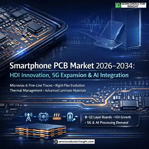
Modern smartphones typically use 8-layer to 12-layer PCBs, compared to 4-layer designs a decade ago. This shift reflects the rising complexity of semiconductor integration.
High-Density Interconnect (HDI) PCBs
HDI PCBs represent the largest and fastest-growing sub-segment within the smartphone PCB market. These boards use microvias, blind vias, and fine-line trace technology to enable dense semiconductor packaging in minimal space.
Flagship smartphones from brands such as Apple, Samsung, and Xiaomi rely heavily on HDI designs to integrate:
- Application processors
- LPDDR memory
- RF front-end modules
- Power management ICs
HDI technology allows manufacturers to reduce board size while increasing functionality, directly supporting ultra-slim smartphone designs.
Rigid, Flexible, and Rigid-Flex PCB Segments
- Rigid PCBs remain essential for mounting core semiconductor components such as processors and memory chips. They provide mechanical stability and precise electrical performance.
- Flexible PCBs (FPCs) are increasingly used for connecting displays, cameras, fingerprint sensors, and battery modules. Their ability to bend and fold supports modern smartphone layouts, including edge-to-edge screens.
- Rigid-Flex PCBs combine both structures, enabling compact interconnections while maintaining high signal reliability. This segment is gaining traction in premium smartphones where space optimization is critical.
Semiconductor Packaging and PCB Co-Design
One of the most important trends shaping the smartphone PCB market is co-design between semiconductor packaging and PCB layout. Advanced packaging formats such as package-on-package (PoP) and system-in-package (SiP) require precise PCB compatibility.
PCBs must now accommodate:
- Ultra-fine pitch solder joints
- Increased I/O density
- Thermal paths for heat-intensive chips
Thermal Management and Power Integrity Challenges
As smartphone processors integrate AI engines, 5G modems, and advanced GPUs, thermal and power challenges have intensified. PCBs play a critical role by incorporating:
- Thicker copper layers for heat spreading
- Dedicated ground planes for noise reduction
- Optimized power distribution networks
Failure in PCB thermal design can lead to performance throttling, reduced battery life, and long-term reliability issues, making this a key focus area for manufacturers.
Materials Innovation in Smartphone PCBs
Material selection has become a competitive differentiator in the smartphone PCB market. Traditional FR-4 substrates are being supplemented or replaced by high-frequency laminate materials that support faster data rates and reduced signal loss.
Advanced resin systems, low-dielectric materials, and improved copper foils are increasingly used to meet semiconductor performance requirements, especially for 5G-enabled devices.
Manufacturing Scale and Supply Chain Dynamics
The smartphone PCB supply chain is highly globalized, with major manufacturing hubs in China, Taiwan, South Korea, and Southeast Asia. Leading PCB manufacturers are investing heavily in automation, yield optimization, and semiconductor-grade quality control.
Production volumes are directly tied to smartphone shipment cycles, making scalability and cost control critical competitive factors.
At Last before Ending, Don’t Forget to Browse Our Recent Exclusive Report for Detailed Insights:
https://semiconductorinsight.com/report/smartphone-pcb-market/
Looking ahead, the smartphone PCB market is expected to benefit from:
- Continued 5G device penetration
- On-device AI processing expansion
- Increased semiconductor content per smartphone
- Growing adoption of foldable and modular phone designs
For competitors, differentiation will depend on HDI expertise, material innovation, and close collaboration with semiconductor designers rather than pure volume manufacturing.
Smartphone PCB market is no longer just an electronics sub-segment—it is a core enabler of semiconductor innovation in mobile devices. As smartphones continue to evolve into high-performance computing platforms, PCB technology will remain central to enabling speed, efficiency, and reliability at scale.
In the semiconductor ecosystem, smartphone PCBs represent the invisible architecture that turns advanced chips into functional, consumer-ready technology.

Comments (0)