
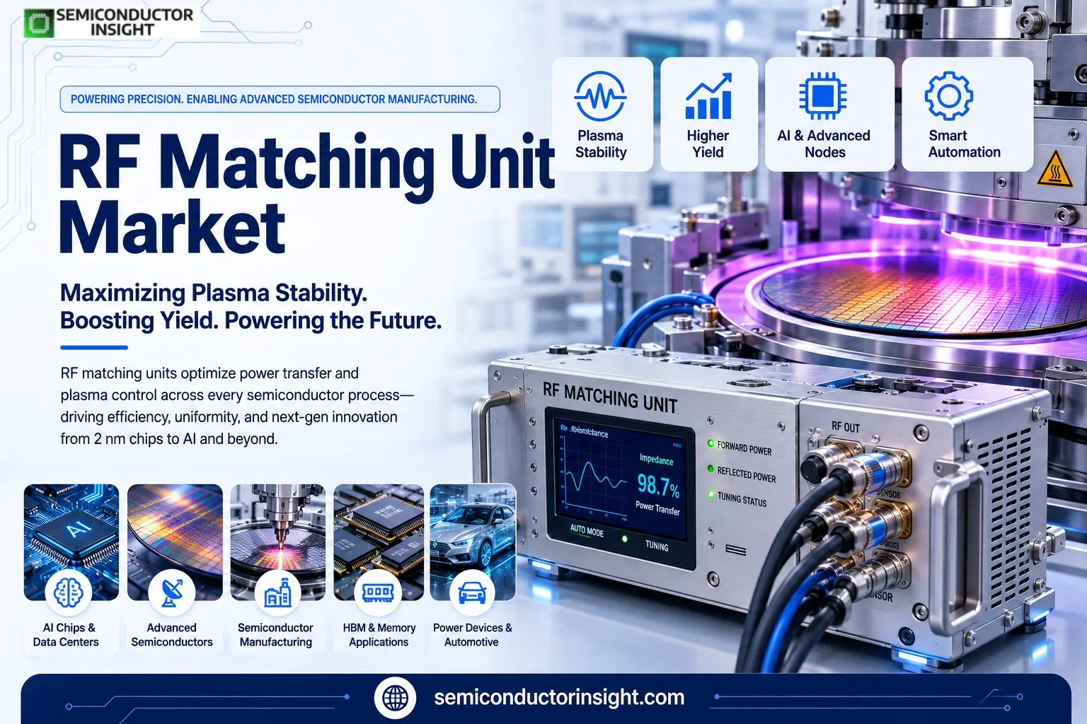
How RF Matching Unit Market Enables Precision Plasma Manufacturing for AI Chips?
As semiconductor manufacturing moves toward 2 nm, gate-all-around (GAA), advanced memory, and heterogeneous packaging, every stage of wafer fabrication requires greater electrical precision than ever before. One technology operating quietly behind these processes is the RF Matching Unit, a critical subsystem that maximizes power transfer between RF generators and plasma chambers used in semiconductor fabrication.
Rather than producing chips directly, RF matching units stabilize plasma by continuously adjusting impedance during etching, deposition, sputtering, ion implantation, and PECVD processes. Their ability to minimize reflected RF power improves wafer uniformity, process repeatability, and equipment productivity. As AI processors, HBM memory, advanced sensors, and power semiconductors become increasingly complex, demand for intelligent RF matching technologies continues to grow across leading fabrication facilities.
Why Precise Plasma Control Has Become a Manufacturing Necessity?
Every advanced semiconductor wafer undergoes hundreds of plasma-based manufacturing steps. During these processes, plasma characteristics change continuously as wafer materials evolve. Without automatic impedance correction, reflected RF energy increases, reducing plasma stability and creating process variations that affect yield.
Modern RF matching units continuously monitor chamber conditions and automatically tune capacitors or inductors within milliseconds, ensuring nearly maximum RF power reaches the plasma. This capability has become particularly important for advanced logic, NAND flash, DRAM, SiC power devices, MEMS sensors, and compound semiconductor manufacturing where dimensional tolerances are measured in only a few nanometers.
According to SEMI, more than 90 new semiconductor fabrication facilities are expected to enter operation globally between 2024 and 2028, significantly increasing demand for plasma processing equipment and associated RF subsystems.
Behind Every AI Chip Is an RF Matching System
- The rapid expansion of artificial intelligence infrastructure has dramatically increased wafer production requirements. Advanced GPUs, AI accelerators, HBM memory stacks, networking processors, and chiplet architectures all require multiple plasma-intensive fabrication stages before packaging.
- TSMC began volume production of 2 nm technology during 2025, while Samsung and Intel continue expanding Gate-All-Around transistor manufacturing. Each process generation introduces increasingly complex plasma recipes requiring highly responsive automatic impedance matching.
- Leading semiconductor equipment manufacturers are integrating digital RF matching systems capable of real-time tuning, predictive diagnostics, and process optimization to support higher wafer throughput with tighter manufacturing tolerances.
Numbers That Explain the Growing Importance of RF Matching Units
Modern semiconductor fabrication facilities process 40,000 to more than 150,000 wafers per month, depending on facility size and technology node. A single advanced wafer can experience over 1,000 individual processing steps, with hundreds involving plasma etching or thin-film deposition where RF matching systems operate continuously.
Advanced plasma tools typically utilize RF power frequencies including 13.56 MHz, 27.12 MHz, 40.68 MHz, and 60 MHz, while high-density plasma reactors may operate at RF power levels ranging from several hundred watts to more than 10 kilowatts depending on application. Even small impedance mismatches can reduce transferred power significantly, making automatic tuning essential for maintaining production consistency.
Global semiconductor manufacturing capacity continues expanding as governments support domestic chip production. According to SEMI and industry announcements, wafer fabrication capacity is expected to exceed 10 million 200 mm equivalent wafers per month globally over the coming years, increasing the installed base of plasma processing systems and RF matching equipment.
Don’t Forget to Surf Our Updated Report for More Detailed Analysis: https://semiconductorinsight.com/report/rf-matching-unit-market/
Digital RF Intelligence Is Replacing Conventional Hardware
- Traditional RF matching units relied primarily on mechanical capacitor adjustments with limited adaptability. Today’s systems integrate digital controllers, high-speed sensors, embedded processors, and machine learning algorithms capable of responding to plasma fluctuations almost instantaneously.
- These intelligent platforms continuously monitor reflected power, impedance, phase angle, and chamber conditions while automatically optimizing matching parameters without interrupting production. Equipment suppliers are also introducing predictive maintenance capabilities that identify component degradation before failures occur, reducing expensive semiconductor fab downtime.
- As fabs become increasingly automated, RF matching units are evolving into connected subsystems capable of communicating directly with factory-wide manufacturing execution systems and process control platforms.
Semiconductor Expansion Is Creating New Opportunities
Recent investments across the global semiconductor industry continue reinforcing long-term demand. TSMC has accelerated construction of new fabrication facilities in Taiwan, Arizona, and Japan. Intel continues expanding manufacturing capacity through projects in the United States and Europe, while Samsung is investing heavily in advanced logic and memory production.
In parallel, governments implementing initiatives such as the US CHIPS and Science Act, the European Chips Act, and semiconductor manufacturing incentives across Japan, South Korea, and India are encouraging construction of additional wafer fabrication facilities. Every new plasma processing chamber installed within these fabs requires highly reliable RF matching technology capable of supporting advanced manufacturing processes.
Innovation Is Moving Beyond Hardware Performance
- The next phase of RF matching technology is increasingly defined by software intelligence rather than mechanical performance alone.
- Manufacturers are incorporating adaptive algorithms, digital twin simulations, AI-assisted plasma optimization, and cloud-based equipment diagnostics to improve process stability and operational efficiency.
- These innovations allow semiconductor manufacturers to achieve higher wafer yields, shorter process qualification times, and more consistent production across increasingly complex technology nodes.
As AI processors, advanced packaging, silicon photonics, wide-bandgap semiconductors, and quantum devices continue pushing fabrication complexity to new levels, RF matching units are becoming one of the indispensable enabling technologies supporting the future of semiconductor manufacturing.

Comments (0)