

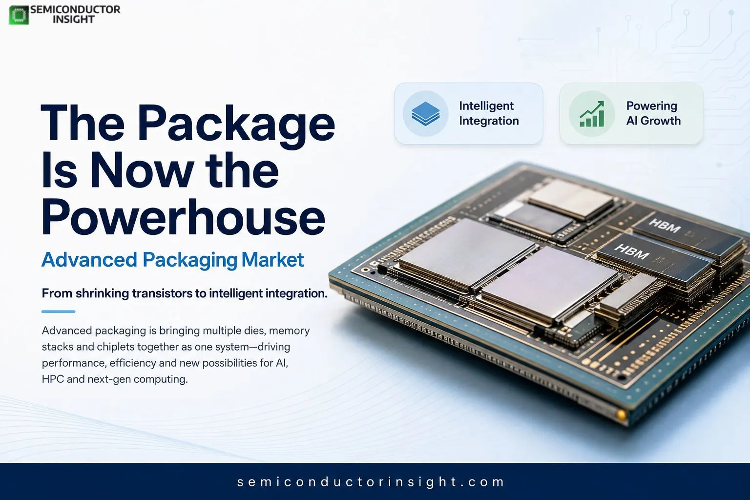
How Is the Advanced Packaging Market Solving the Limits of Conventional Monolithic Chips?
For decades, semiconductor progress was closely associated with shrinking transistor dimensions. That equation is changing. As AI accelerators, high-performance computing processors and networking devices require enormous amounts of processing power and memory bandwidth, the package itself has become a major part of system architecture.
Advanced packaging brings multiple dies, chiplets, memory stacks and interconnect structures together so they can operate as one system. Technologies such as 2.5D integration, 3D stacking, chiplets, silicon interposers, hybrid bonding and fan-out packaging are consequently becoming central to semiconductor engineering.
TSMC reported that advanced technologies at 7-nanometer and below represented 74% of its total wafer revenue in 2025, while the company manufactured 12,682 products for 534 customers. Its packaging roadmap includes CoWoS, InFO and SoIC technologies.
AI Is Changing What Engineers Expect From a Package
The growth of AI computing has created a packaging problem that cannot be solved simply by producing a larger monolithic die. Large AI processors increasingly combine compute dies with high-bandwidth memory and other specialized components.
The architecture can be viewed as:
Compute dies → High-bandwidth memory → Interconnect structure → Advanced substrate → Complete AI package
The closer these components can be placed and the more efficiently they can communicate, the greater the potential improvement in bandwidth, latency and energy efficiency.
This is why HBM integration and chiplet architectures have become closely associated with the latest generation of AI hardware.
Chiplets Turn Packaging Into an Architecture Decision
- Chiplets are changing the role of packaging from a final manufacturing step into something considered much earlier during chip design. Instead of building every function into one enormous piece of silicon, designers can combine specialized dies within one package.
- Intel is using Foveros 3D stacking and EMIB embedded-bridge technology for this approach. In July 2026, Intel described its New Mexico advanced-packaging operations as scaling packages to approximately 8 times the industry’s standard reticle limit today, with a target of more than 12 times by 2028. The facility has around 2,700 employees and 500 suppliers.
- That illustrates the scale of change: packaging is increasingly being used to overcome physical limitations that conventional single-die architectures cannot easily address.
Inside the US Packaging Race
Which companies are pioneers in advanced packaging technology in the United States?
- The United States has several major technology contributors, with Amkor standing out for domestic manufacturing and packaging capabilities, while TSMC is rapidly expanding its US footprint through Arizona investments.
- Amkor is building a large-scale advanced packaging and test campus in Arizona, while TSMC is integrating advanced manufacturing and planned packaging capabilities into its expanding US ecosystem.
- Amkor announced a planned $7 billion investment across two phases for its Arizona campus. The project is expected to provide more than 750,000 square feet of cleanroom space and up to 3,000 jobs, with first production expected in early 2028.
- The development became even more significant in June 2026, when TSMC and Amkor announced a 10-year agreement to expand advanced packaging and testing capabilities in Arizona.
To find out more, feel free to browse our latest updated related report: https://semiconductorinsight.com/report/advanced-packaging-chip-last-level-cache-sram-macro-market/
Packaging Capacity Is Becoming a Strategic Asset
The investment cycle demonstrates how packaging is moving closer to the center of national semiconductor strategies. TSMC announced in 2025 that its planned US investment could reach $165 billion, including three additional fabs, two advanced packaging facilities and an R&D center.
Amkor’s 2025 financial performance also provides a useful industry signal. The company reported $6.71 billion in full-year revenue, with advanced packaging and computing revenue reaching record levels.
These developments indicate that packaging capacity is increasingly being treated as critical infrastructure rather than simply outsourced back-end manufacturing.
Hybrid Bonding Pushes Interconnects Into the Micron Scale
One of the most technically important developments is hybrid bonding, which enables extremely fine-pitch connections between stacked dies. Intel has disclosed Foveros Direct technology with hybrid-bonding interconnect pitches of less than 5 micrometers for its advanced packaging roadmap.
At these dimensions, alignment accuracy, thermal management, yield and inspection become critical engineering considerations. The commercial value therefore extends beyond packaging equipment into bonding materials, substrates, inspection systems, thermal solutions and semiconductor manufacturing software.
The Next Packaging Bottleneck Is Not Just Silicon
- Advanced packaging is creating a wider semiconductor ecosystem.
- As packages become larger and more complex, manufacturers must coordinate thermal dissipation, power delivery, signal integrity, warpage control, substrate design and high-density interconnects.
- That creates opportunities across the semiconductor supply chain, from advanced substrates and interposers to bonding equipment, materials and testing systems.
- The market is consequently entering a phase where the question is no longer simply how small a transistor can become.
- The more important question is how many useful computing elements can be assembled, connected and cooled inside one intelligent package.
That shift is positioning advanced packaging as one of the defining technologies behind the next generation of AI accelerators, high-performance computing systems and increasingly heterogeneous semiconductor architectures.

Comments (0)