
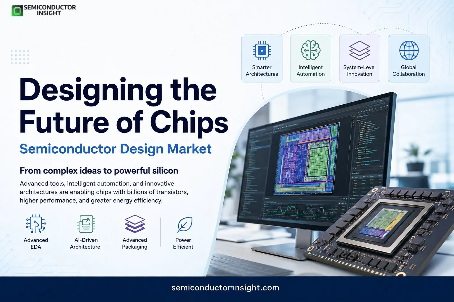
How Are Semiconductor Design Teams Navigating Transistor Counts in the Billions Today?
Semiconductor design sits at the heart of modern electronics, where engineers craft the blueprints for chips powering everything from smartphones to data centers and advanced AI systems. This domain encompasses everything from high-level architecture to physical layout, relying heavily on electronic design automation (EDA) software to manage unprecedented complexity.
Current stuies transistor count records show modern processors reaching 184 billion transistors in devices like Apple’s M3 Ultra SoC fabricated on 3 nm processes, illustrating the scale designers must handle.
The Transistor Density Revolution Reshaping Design Workflows
- Chip designs have evolved dramatically, with a single square millimeter now capable of housing around 200 million transistors.
- A standard 300 mm wafer can incorporate trillions across thousands of individual dies.
- Design teams use sophisticated IP cores and modular architectures to integrate billions of these switches efficiently, balancing power, performance, and area constraints.
- This density surge demands advanced verification methods to ensure functionality before costly fabrication.
EDA Tools and the Design Automation Landscape
Electronic design automation platforms have become indispensable, handling simulation, synthesis, and physical implementation for intricate SoCs. Current workflows incorporate machine learning algorithms to optimize routing and placement, reducing design cycles that once took months.
Case studies from major foundries highlight how these tools manage multi-die systems and 3D stacking, allowing integration of diverse functions like processors, memory, and accelerators on one package.
AI and Machine Learning Integration in Chip Architecture
Ongoing examples show semiconductor design shifting toward specialized AI accelerators. Companies are developing chips with dedicated tensor cores and neural processing units, as seen in recent data center processors optimized for large language models.
Design teams incorporate heterogeneous computing approaches, mixing CPU, GPU, and custom accelerators to achieve energy efficiency gains critical for edge and cloud applications. Global data center expansion drives demand for these tailored designs, with chips processing vast datasets in real time.
Advanced Packaging and System Level Co Design
Semiconductor design now extends beyond individual dies to encompass advanced packaging techniques like chiplets and 2.5D/3D integration. This co-design philosophy treats the package as an extension of the chip, requiring new tools for thermal modeling and signal integrity across interfaces.
Recent implementations in high-performance computing demonstrate how these methods overcome traditional scaling limits, enabling higher bandwidth and lower latency in systems handling exascale computations.
For More Detailed Insights, You Can Surf Our Latest Report Here: https://semiconductorinsight.com/report/semiconductor-design-market/
- IP Reuse and Modular Design Strategies
- Intellectual property blocks form building blocks for faster time-to-market. Designers license processor cores, interface standards, and security modules, then customize them for specific applications.
- This modular approach appears prominently in automotive and mobile sectors, where safety-certified IP integrates with custom logic.
- Government initiatives worldwide support domestic design capabilities through funding for R&D in secure and resilient architectures.
- Power Efficiency Challenges in Next Generation Nodes
- As process nodes advance, design focuses intensely on power management. Techniques such as dynamic voltage scaling, clock gating, and near-threshold computing help control consumption in chips with tens of billions of transistors.
- Mobile and IoT designs particularly emphasize this, resulting in SoCs that deliver high performance within tight battery and thermal budgets.
- Data from industry reports indicate these optimizations enable deployment in diverse environments from wearables to infrastructure.
Verification and Testing Innovations for Complex Systems
With rising complexity, verification consumes a large portion of design resources. Teams employ formal methods, emulation, and hardware-in-the-loop testing to validate functionality across billions of possible states.
Ongoing projects in quantum-resistant cryptography and real-time safety systems showcase how rigorous verification prevents costly post-silicon bugs. Magazines covering semiconductor engineering frequently detail how these practices ensure reliability in mission-critical applications like autonomous vehicles and medical devices.
Global Collaboration and Talent Development in Design
Semiconductor design thrives on international knowledge sharing, with teams distributed across continents collaborating via cloud-based EDA environments. Educational programs and research institutions contribute by training engineers in emerging areas like photonic integration and neuromorphic computing.
Current scenarios reflect heightened activity in response to supply chain dynamics, spurring investments in design talent and infrastructure to maintain innovation pace.
Sustainability Considerations in Modern Design Flows
Designers increasingly factor environmental impact into choices around materials and architectures. Low-power designs reduce operational carbon footprints, while recyclable packaging and efficient manufacturing considerations gain traction. Initiatives promote longer chip lifecycles through upgradable architectures, aligning semiconductor innovation with broader ecological goals.
Semiconductor design market continues pushing boundaries of what’s possible in electronics, with each generation building on the last to deliver greater capabilities in smaller, more efficient forms.

Comments (0)