

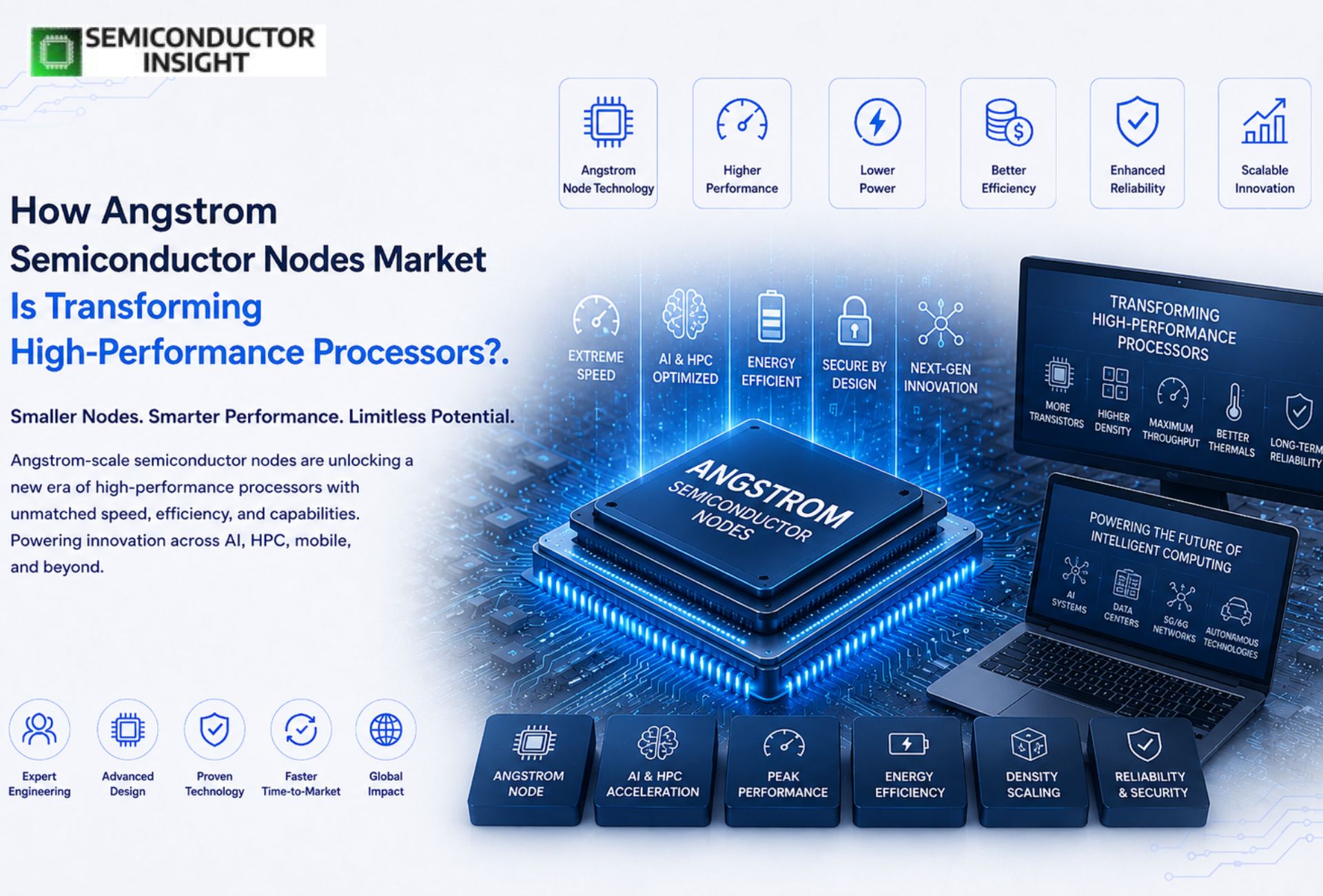
How Angstrom Semiconductor Nodes Market Is Transforming High-Performance Processors?
Angstrom Semiconductor Nodes Market refers to the semiconductor industry segment focused on developing and manufacturing ultra-advanced chip fabrication technologies measured in angstroms (Å), where 1 angstrom equals 0.1 nanometers.
These nodes represent the next generation of semiconductor process technologies beyond traditional nanometer-based naming systems such as 7nm, 5nm, and 3nm.
An angstrom equals 0.1 nanometres, and while commercial chips are not literally measured in angstrom units yet, major foundries are using the term to describe technologies beyond the 2 nm generation. Companies are positioning these nodes as the gateway to ultra-dense transistor architecture with lower power leakage and higher processing efficiency.
Feel Free to Reach Our Most Recent Updates of the Relevant Report: https://semiconductorinsight.com/report/advanced-packaging-for-ai-chip-market/
Atomic Scale Manufacturing Becomes the New Battleground
- The semiconductor race has shifted from simple transistor shrinkage to atomic-level material engineering. Manufacturers are increasingly adopting Gate All Around transistor structures instead of traditional FinFET designs. These advanced architectures allow tighter control over current leakage and improve performance for AI-intensive workloads.
- In 2025, Samsung Electronics accelerated development around its 2 nm and future angstrom-class roadmap, while Taiwan Semiconductor Manufacturing Company continued pilot work on advanced process technologies targeting AI accelerators and data centre Intel Corporation has also invested heavily in its 18A process node, where the A represents angstrom-class branding rather than a direct physical measurement.
- The transition is capital-intensive. A single High Numerical Aperture EUV lithography machine from ASML can cost more than USD 350 million, making advanced node manufacturing one of the most expensive industrial activities globally.
AI Servers Push Demand for Denser Chip Architectures
Generative AI has radically changed semiconductor priorities. Training large language models requires processors with enormous transistor density and lower energy consumption. Advanced angstrom-class nodes are becoming essential for AI GPUs, AI accelerators, and cloud inference chips.
According to publicly available semiconductor industry data, hyperscale data centre electricity consumption could surpass 1,000 terawatt-hours annually before the end of the decade due to AI expansion. This has intensified the need for chips that can deliver higher compute output per watt.
Modern AI processors already contain more than 150 billion transistors on a single package. Some advanced semiconductor packages integrate multiple chiplets connected through ultra-high bandwidth interconnects, creating computing platforms capable of processing trillions of operations per second.
The Rise of High NA EUV Lithography
- One of the biggest enablers for angstrom-scale nodes is high-NA EUV lithography. Traditional lithography systems struggle to print increasingly compact transistor features with acceptable yields. High NA systems improve resolution and reduce patterning complexity.
- Early High NA tools weigh more than 150 metric tons and require thousands of precision-engineered components. Semiconductor fabs deploying these systems are redesigning entire cleanroom layouts to accommodate the machines.
- The Netherlands-based equipment ecosystem has become strategically important because advanced lithography access now influences global semiconductor leadership. Governments across the United States, South Korea, Japan, and the European Union are expanding domestic chip manufacturing incentives to secure next-generation production capabilities.
Smartphone Brands Are Quietly Preparing for the Angstrom Era
While AI infrastructure dominates headlines, consumer electronics companies are equally focused on angstrom-class chips. Premium smartphones increasingly require processors capable of handling on-device AI image generation, real-time language translation, and advanced gaming graphics without overheating.
Flagship processors launching in the coming years are expected to integrate more advanced transistor stacking methods and backside power delivery systems. These changes could significantly improve battery efficiency while increasing processing throughput.
Foldable devices, mixed reality headsets, and AI PCs are also driving interest in compact and energy-efficient semiconductor nodes. Industry engineers are exploring new materials, including ruthenium interconnects and 2D semiconductor compounds, to overcome physical scaling limitations.
Packaging Innovation Is Becoming More Important Than Node Size
The market is no longer focused only on smaller transistors. Advanced packaging technologies now play an equally important role in semiconductor performance.
- Chiplet architecture allows manufacturers to combine multiple specialised chips into one integrated package. This approach improves scalability while reducing manufacturing costs associated with monolithic die production.
Several AI accelerators now use 3D stacked memory systems capable of transferring data at speeds exceeding 1 terabyte per second. These packaging breakthroughs are helping semiconductor companies continue performance growth even as traditional Moore’s Law scaling becomes increasingly difficult.
University Labs and National Programs Are Shaping the Next Leap
Research institutions are becoming central contributors to Angstrom Semiconductor Nodes market. Universities and government-backed laboratories are investigating atomic layer deposition, nanosheet transistors, and quantum-compatible semiconductor materials.
The United States CHIPS and Science Act has allocated tens of billions of dollars toward semiconductor manufacturing and research initiatives. Japan and Europe are also funding advanced semiconductor pilot lines to reduce dependency on external manufacturing ecosystems.
This global race is no longer only about commercial electronics. Semiconductor capability now influences defence systems, telecommunications infrastructure, medical computing, and national AI competitiveness.
The Semiconductor Industry Is Entering a Physics-Driven Decade
Angstrom Semiconductor Nodes market represents more than another manufacturing milestone. It signals a transition where semiconductor progress depends on breakthroughs in materials science, atomic engineering, and advanced packaging integration.
As transistor structures approach physical limitations, innovation is increasingly shaped by how efficiently companies can manipulate matter at near-atomic dimensions. The next decade of computing performance may depend less on traditional scaling and more on how effectively the semiconductor industry combines lithography, packaging, AI optimisation, and material innovation into one unified ecosystem.

Comments (0)