
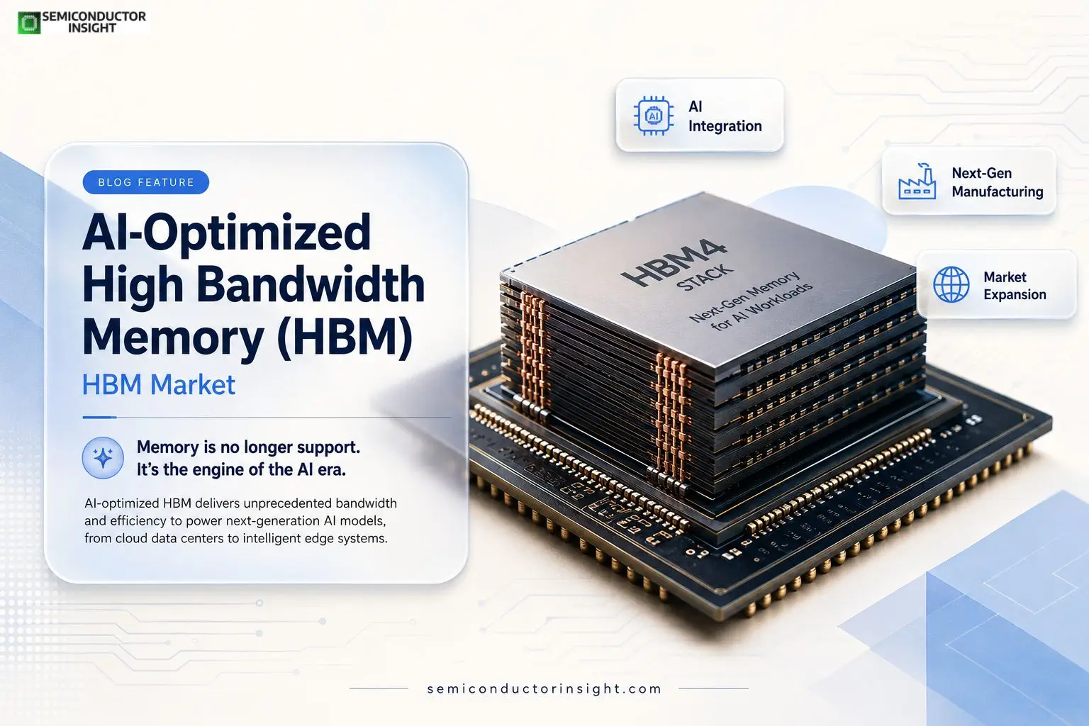
HBM4 vs. HBM3E in the AI-Optimized High Bandwidth Memory (HBM) Market Which Technology Leads AI Training?
Artificial intelligence has transformed memory from a supporting component into one of the most strategic assets in semiconductor manufacturing. As foundation models become larger and AI inference expands into cloud services, autonomous systems, healthcare, robotics, and industrial automation, memory bandwidth has become just as important as computing power. AI-Optimized High Bandwidth Memory (HBM) is emerging as the preferred architecture because it enables GPUs and AI accelerators to process enormous datasets while reducing latency and improving energy efficiency.
The demand surge is no longer driven only by hyperscale cloud providers. National AI initiatives, sovereign AI infrastructure, enterprise AI deployment, and custom AI chips are expanding HBM adoption worldwide. The transition from HBM3E to HBM4 represents more than a product upgrade it reflects the industry’s move toward memory designed specifically for trillion-parameter AI models.
AI Factories Are Creating a New Memory Economy
- The rise of AI factories is changing how semiconductor companies prioritize memory production. Instead of supplying general-purpose DRAM, manufacturers are allocating wafer capacity specifically for HBM stacks integrated with advanced packaging technologies.
- According to the Semiconductor Industry Association (SIA), worldwide semiconductor sales reached approx. USD 627.6 billion in 2024, the industry’s highest annual revenue ever recorded. Memory products accounted for the fastest-growing category, supported by AI server deployments.
- Modern AI servers may integrate 8 to 12 HBM stacks around a single accelerator using advanced 2.5D packaging. An HBM4 stack is expected to deliver bandwidth exceeding 2 terabytes per second, enabling significantly larger AI models to remain in memory during training.
- Meanwhile, TSMC’s CoWoS advanced packaging capacity continues expanding to address unprecedented AI accelerator demand, illustrating that packaging capacity has become nearly as valuable as silicon fabrication itself.
Why Memory Architecture Has Become the Real AI Performance Multiplier
For years, semiconductor innovation focused primarily on transistor scaling. Today’s AI workloads reveal a different limitation moving data efficiently between processors and memory.
HBM addresses this challenge through vertically stacked DRAM connected with thousands of Through-Silicon Vias (TSVs). This architecture dramatically shortens data travel distances while delivering far greater bandwidth than conventional server memory.
The result extends beyond faster AI training. Large language models experience lower latency, AI inference becomes more energy efficient, recommendation systems respond faster, and scientific simulations process increasingly complex datasets. As GPU performance accelerates with every generation, memory bandwidth increasingly determines real-world system performance.
From Chip Packaging to National AI Strategies
Governments are increasingly treating advanced memory manufacturing as strategic infrastructure rather than a conventional semiconductor business.
Countries including the United States, South Korea, Japan, and members of the European Union continue investing in semiconductor manufacturing ecosystems that combine wafer fabrication, advanced packaging, AI computing, and supply chain resilience.
At the same time, cloud providers continue announcing multi-billion-dollar AI data center expansions requiring thousands of GPU clusters. Each deployment significantly increases demand for HBM, advanced substrates, packaging equipment, and thermal management technologies, creating ripple effects across the semiconductor value chain.
Inside the Latest HBM4 Pricing Signals and Supply Negotiations
- The latest industry reporting indicates that commercial discussions surrounding HBM4 remain highly dynamic as qualification programs accelerate ahead of broader production.
- Recent reports from semiconductor trade publications suggest that HBM4 pricing is currently being negotiated at an estimated premium of roughly 20% to 30% over comparable HBM3E products, reflecting its higher bandwidth, larger die configurations, more advanced packaging requirements, and stronger AI performance expectations.
- Among leading suppliers, SK hynix continues to maintain a strong position through early customer engagements, while Samsung Electronics and Micron Technology are expanding qualification activities with major AI accelerator developers.
- Rather than publicly announcing fixed unit prices, vendors are reportedly negotiating long-term supply agreements tied to production volumes, packaging availability, and customer roadmaps.
- Industry commentary published within the past day also points to continued tight supply planning rather than excess inventory. Procurement discussions increasingly focus on guaranteed allocation, yield improvement, and advanced packaging capacity instead of short-term price reductions.
- Buyers are prioritizing secure multi-year supply commitments as demand from hyperscale AI infrastructure continues to outpace available manufacturing capacity.
Growth Indicators Reflect the Increasing Strain on AI Memory Production
Several measurable indicators demonstrate the pace of change.
JEDEC’s latest HBM standards continue increasing memory density and bandwidth generation after generation. A single AI accelerator equipped with HBM can access memory bandwidth measured in terabytes per second, several times greater than conventional DDR server memory.
Modern AI clusters often deploy thousands of GPUs interconnected across large-scale data centers, with each accelerator requiring multiple HBM stacks. Industry analysts and semiconductor manufacturers estimate that HBM output remains constrained primarily by advanced packaging capacity rather than wafer production alone, making CoWoS expansion one of the semiconductor industry’s highest priorities.
For a more thorough report, please contact us using our most recent report: https://semiconductorinsight.com/report/ai-optimized-high-bandwidth-memory-hbm-market/
Why the Next AI Breakthrough May Depend More on Memory than Compute?
The AI era is redefining the semiconductor hierarchy. Instead of viewing memory as a supporting component, system designers increasingly treat HBM as a core performance enabler that determines AI scalability, efficiency, and deployment economics. As HBM4 enters commercial production and advanced packaging ecosystems expand, AI-optimized memory will continue shaping everything from hyperscale computing to edge AI systems, making it one of the defining technologies behind the next generation of semiconductor innovation.

Comments (0)