
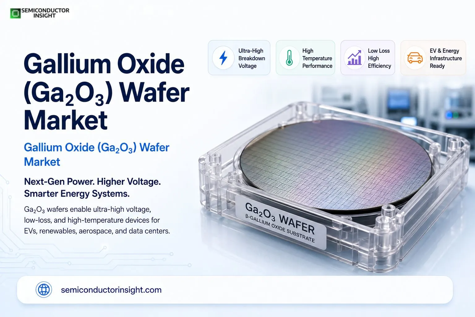
Growing Importance of the Gallium Oxide Ga2O3 Wafer Market in Aerospace Electronics Systems
Gallium oxide wafers are moving from laboratory-scale experimentation toward serious industrial semiconductor discussions. As power electronics manufacturers search for materials capable of operating at higher voltages, lower losses, and extreme temperatures, gallium oxide (Ga2O3) is gaining recognition as one of the most promising ultra-wide bandgap semiconductor materials currently under development.
Unlike conventional silicon substrates, Ga2O3 wafers are engineered for high breakdown electric fields, enabling semiconductor devices to handle significantly higher voltages while maintaining energy efficiency. Researchers and semiconductor fabrication companies are increasingly exploring this material for electric vehicles, renewable energy systems, aerospace electronics, industrial motor drives, and high-frequency communication infrastructure.
Power Electronics Research Is Expanding Beyond Silicon Carbide
For years, silicon carbide and gallium nitride dominated discussions around advanced power semiconductors. However, gallium oxide is attracting new attention because of its exceptionally high theoretical breakdown field strength, which researchers estimate to be nearly eight megavolts per centimeter.
This property allows semiconductor devices built on Ga2O3 wafers to potentially operate with thinner layers and lower resistance compared to conventional wide-bandgap materials.
Material Comparison Snapshot
The approximate band gap varies significantly across semiconductor materials, which directly influences their electrical performance and suitability for different applications. Silicon has a band gap of around 1.1 eV, making it the most widely used material in conventional electronics.
Gallium Nitride offers a much wider band gap of about 3.4 eV, while Silicon Carbide is close behind at approximately 3.3 eV. Gallium Oxide stands out with the widest band gap in this group, ranging from 4.8 to 4.9 eV, which makes it especially promising for high-power and high-voltage applications.
Research data published through the U.S. Naval Research Laboratory and Japanese semiconductor institutes continues to highlight the potential of gallium oxide for ultra-high voltage switching applications.
Electric Vehicle Charging Systems Are Driving Experimental Demand
One of the most active research areas for Ga2O3 wafers involves electric mobility infrastructure. Ultra-fast charging systems require semiconductor devices capable of managing high-power conversion while minimizing thermal losses.
Several university-led semiconductor programs in Japan, Germany, and the United States are studying gallium oxide transistors for EV charging modules and traction inverter systems. These projects are exploring how Ga2O3 devices could reduce cooling requirements and improve charging efficiency in high-voltage automotive systems.
To Know More about the Report, You Can Freely Browse Our Latest Updated Report: https://semiconductorinsight.com/report/gallium-oxide-gao-wafer-market/
Emerging EV Semiconductor Stack
Battery System
↓
Power Conversion Module
↓
Ga2O3-Based Switching Device
↓
Fast Charging Output
This structure is becoming increasingly important as electric vehicle platforms move toward 800-volt architectures and megawatt-scale charging systems.
Crystal Growth Technologies Are Becoming a Key Industry Focus
Scientific and industry interest in the wafer fabrication process itself is growing. Gallium oxide can be made using melt-growth processes, which may eventually reduce manufacturing costs, in contrast to certain modern semiconductor materials that need extremely complex fabrication procedures.
Researchers are currently developing larger-diameter Ga2O3 wafers to improve scalability for industrial semiconductor fabrication. Crystal growth laboratories in Japan and Europe have successfully demonstrated two-inch and four-inch beta gallium oxide substrates for experimental device development.
Current Wafer Development Activity
| Development Area | Industry Focus |
| Larger substrate diameters | Improved fabrication scalability |
| Defect density reduction | Better device reliability |
| Thermal management structures | Heat dissipation improvement |
| Epitaxial layer optimization | Higher power efficiency |
Several semiconductor research centres are also working on hybrid substrate integration methods that combine gallium oxide layers with advanced cooling materials to address thermal conductivity limitations.
Data Centers Are Creating Interest in High-Efficiency Switching Devices
- AI infrastructure and hyperscale data centres are increasing demand for more energy-efficient power systems. Data centers consume enormous electricity volumes due to server operations and cooling requirements.
- According to the International Energy Agency, global data center electricity consumption exceeded 460 terawatt-hours annually in recent years. This growing power demand is encouraging semiconductor researchers to investigate next-generation switching materials capable of reducing electrical losses in power delivery systems.
- Gallium oxide devices are being evaluated for high-frequency switching applications that may improve efficiency in server power supplies, industrial converters, and energy distribution architectures used inside AI computing facilities.
Aerospace and Defense Programs Are Expanding Material Research
Ga2O3 wafers are also drawing interest from aerospace and defense electronics developers because ultra-wide bandgap materials can support operation under extreme environmental conditions.
Satellite systems, radar electronics, and advanced aviation platforms often require semiconductors capable of functioning in high-radiation and high-temperature environments. Research collaborations involving government laboratories and university semiconductor programs are exploring gallium oxide devices for these applications.
In 2025, several semiconductor conferences in the United States and South Korea highlighted experimental Ga2O3 transistor demonstrations designed for high-power radar modules and aerospace-grade switching systems.
Semiconductor Supply Chains Are Looking Beyond Traditional Materials
The semiconductor industry is increasingly searching for alternative material ecosystems that can complement or outperform existing silicon-based infrastructure. Gallium oxide is becoming part of broader discussions surrounding power grid modernization, industrial electrification, and renewable energy conversion systems.
Renewable Energy Input
↓
Power Conversion Hardware
↓
Ga2O3 Semiconductor Layer
↓
High-Efficiency Energy Transmission
As governments continue investing in electrification projects and advanced semiconductor research funding, gallium oxide wafer development is expected to remain one of the most closely watched experimental areas in power electronics engineering.

Comments (0)