
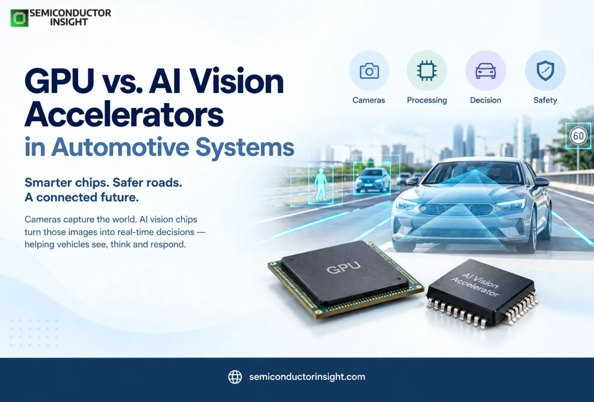
GPU vs. AI Vision Accelerators in Automotive Systems 2026: Understanding the Compute Architecture Shift
A modern vehicle can now process an enormous stream of visual information before a driver has time to react. Cameras identify lanes, vehicles, pedestrians, signs and road markings, while specialized semiconductor architectures convert those images into decisions. This is turning the AI vision system chips market into a crucial part of the broader software-defined vehicle transition.
From Camera Sensor to Machine Perception
- The important shift is no longer simply adding more cameras. The semiconductor must transform raw pixels into useful information with extremely low latency and within strict automotive power and safety limits.
Camera → Image signal processing → Neural-network acceleration → Object detection → Scene interpretation → Vehicle response
- Tesla states that its FSD Supervised system uses eight external cameras covering a 360-degree field of view and processes more than 1 million pixels of visual data every millisecond.
- That workload explains why ordinary processors are increasingly being supplemented or replaced by dedicated AI accelerators, neural-processing engines and heterogeneous SoCs.
The Compute Race Has Moved Into the Car
The scale of automotive AI computing is changing rapidly. NVIDIA’s DRIVE AGX Thor platform is specified at more than 1,000 INT8 TOPS, while DRIVE AGX Orin reaches up to 254 TOPS. NVIDIA’s Hyperion architecture can combine two Thor systems and support configurations involving 14 cameras, nine radars, one lidar and 12 ultrasonic sensors.
These numbers illustrate a broader architectural change: perception is increasingly being handled by centralized computing platforms rather than a collection of isolated electronic control units.
Why Multicamera Processing Is Becoming the New Normal?
Automotive vision systems are moving from single-camera functions such as lane departure warning toward synchronized interpretation of multiple camera feeds.
Qualcomm’s Snapdragon Ride Pilot illustrates this transition. Its perception architecture can scale from single-camera active-safety applications toward systems using 11 or more cameras and five or more radars for higher-tier driving functions. The company says its perception stack has been trained using more than 1 million miles of data collected across more than 100 countries.
This creates demand for chips capable of simultaneously handling image processing, sensor fusion, neural-network inference, memory movement and safety workloads.
Tesla Shows What Vision-Centric Computing Looks Like
- Tesla provides one of the most recognizable examples of vertically integrated automotive vision computing. The company says it began developing its computer-vision technology internally in 2016 and subsequently developed custom silicon for neural-network workloads.
- Its current FSD documentation describes eight high-resolution external cameras and custom Tesla computing hardware processing the surrounding environment. Tesla also emphasizes that its vehicles still require active driver supervision and are not fully autonomous.
- The semiconductor implication is significant: AI vision is becoming a first-class automotive compute workload rather than a software feature added after hardware design.
Does Tesla Use Silicon Carbide?
Yes, but the answer needs to be separated from AI vision computing.
Silicon carbide is primarily associated with Tesla’s power electronics rather than its AI vision processor. The clearest documented example is the Model 3 traction inverter. A teardown of the Model 3 inverter identified 24 STGK026 SiC FETs, arranged in the vehicle’s inverter power stage.
STMicroelectronics also describes SiC MOSFETs as a technology for improving efficiency, size and weight in EV traction-inverter applications.
This distinction matters:
AI vision chips → perception and neural-network computation
SiC power semiconductors → battery-to-motor power conversion
A vehicle can therefore use both technologies for completely different functions.
You Can Freely Surf Our Latest Updated Report Here: https://semiconductorinsight.com/report/ai-vision-system-chips-market/
The 2026 BMW Example Shows Where Architectures Are Heading
BMW’s Neue Klasse iX3 provides another current example of centralized automotive AI computing. Qualcomm says its Snapdragon Ride-based automated-driving system combines 8-megapixel and 3-megapixel cameras with radar and centralized computing, delivering 20 times the computing power of the previous generation. The system debuted at IAA Mobility 2025, with the platform validated in 60 countries and targeted for availability in more than 100 countries by 2026.
The direction is increasingly clear: cameras are becoming richer, AI models are becoming more demanding, and the semiconductor architecture has to process the resulting information locally.
The Next Chip Requirement Is Not Just More TOPS
Raw AI performance is only one part of the equation. Future automotive vision chips also have to balance memory bandwidth, thermal limits, functional safety, redundancy, latency and software compatibility.
The emerging architecture can be viewed as:
More cameras + higher resolution → More visual data → Larger AI models → Greater edge compute → Centralized automotive SoCs → Continuous software updates
Qualcomm’s 2026 collaboration with Wayve further demonstrates this direction, combining production-oriented ADAS/automated-driving software with Snapdragon Ride platforms for applications ranging from hands-off assistance toward more advanced automated driving.
For semiconductor manufacturers, the opportunity therefore extends beyond selling an image processor. The competitive technology is increasingly the complete vision-compute platform capable of turning billions of pixels into usable vehicle intelligence within milliseconds.

Comments (0)