

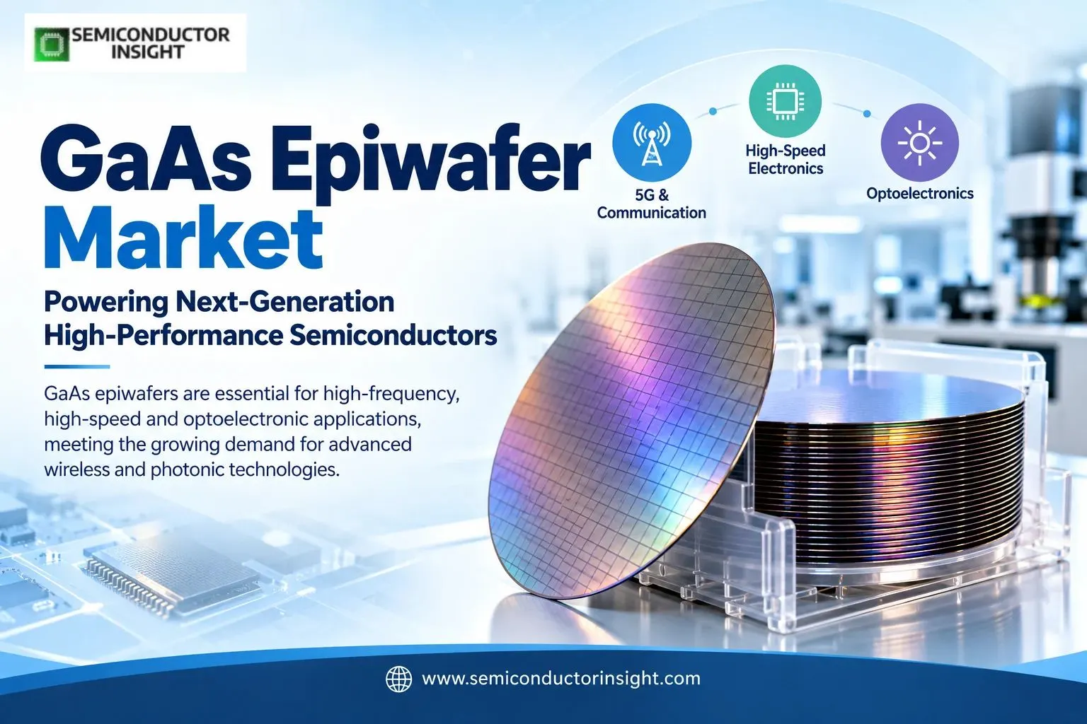
GaAs Epiwafer Market 2026: From 6-Inch Production to 200 mm Platforms for RF and Photonic Devices
Gallium arsenide is no longer confined to a narrow compound-semiconductor niche. Its combination of high electron mobility, high-frequency performance and optoelectronic capability continues to make GaAs an important material platform for RF front ends, VCSELs, laser devices, sensing systems and wireless infrastructure.
- In 2026, GaAs Epiwafer Market is gaining a broader technology footprint as epitaxial structures move into newer generations of connectivity and photonic hardware.
Why the Epiwafer Layer Matters More Than It Looks?
An epiwafer is not simply a polished semiconductor wafer. It contains carefully engineered crystalline layers grown on a substrate, with thickness, composition, doping and interfaces controlled according to the eventual device architecture.
For GaAs, that precision supports technologies including pHEMTs, HBTs, PIN and Schottky diodes, VCSELs and laser structures. IQE currently lists GaAs epiwafer structures spanning RF devices, 850 nm, 940 nm and 1060 nm VCSELs, quantum-well photodetectors and red laser technologies.
This makes epitaxy one of the earliest points at which semiconductor performance is effectively engineered into the material.
The 5G Handset Connection Has Not Disappeared
- GaAs continues to occupy an important position inside wireless front-end architectures.
- High-frequency GaAs HBT and related structures have historically been used for handset power amplifiers because they provide the electrical characteristics required for compact RF systems.
- IQE reported in its 2025 results that it had secured new design wins for 5G mobile handset power-amplifier applications, potentially extending across multiple future device generations.
- The relevance also extends beyond smartphones. GaAs epitaxy supports RF components for Wi-Fi and wireless infrastructure, keeping demand connected to the continuing expansion of high-speed wireless networks.
Larger Wafers Are Changing the Manufacturing Equation
Wafer diameter is becoming an important part of the GaAs story. Sumitomo Electric has documented mass-production capability for conductive and semi-insulating GaAs substrates in 3-, 4- and 6-inch diameters. Its work on 6-inch GaAs substrates was particularly linked to the scaling of VCSEL production.
IQE now states that its GaAs epitaxy can scale to 200 mm, demonstrating how compound-semiconductor manufacturing is moving toward larger formats where application economics justify the transition.
3-inch GaAs → 4-inch production → 6-inch platforms → 200 mm scalable epitaxy → higher device output per manufacturing cycle
The transition is significant because larger substrates can improve wafer utilization and support increasingly sophisticated device architectures.
VCSELs Give GaAs a Second Technology Identity
The GaAs epiwafer story extends well beyond RF. VCSELs have become an important application for GaAs epitaxy because their structures can be engineered for optical sensing and communication.
IQE identifies 3D sensing, optical communications, laser diodes and photodetectors among its GaAs applications. The company also reported qualification and production ramp of second-generation 3D-sensing VCSEL products for a leading global smartphone platform.
This creates a particularly interesting demand chain:
GaAs substrate → Epitaxial layer stack → VCSEL → 3D sensing / optical communication → Smartphone, automotive or data infrastructure
You Can Freely Surf Our Latest Updated Report Here: https://semiconductorinsight.com/report/gaas-epiwafer-market/
AI Data Centers Are Opening an Unexpected GaAs Avenue
The newest development is the connection between GaAs epitaxy and AI infrastructure. In September 2026, IQE announced an agreement with Quintessent to supply 6-inch GaAs epiwafers for quantum-dot laser technology intended for AI data-center optical interconnects. The programme is progressing toward customer sampling and commercial deployment.
This is important because AI data centers are increasing the need for high-speed optical communication between computing systems. The GaAs platform can therefore participate not only in the wireless side of semiconductor demand but also in the optical layer connecting high-performance computing infrastructure.
Satellite and High Frequency Systems Add another Demand Channel
- The wider RF ecosystem is also expanding toward satellite connectivity and mmWave systems.
- In August 2026, AmpliTech announced three design wins involving custom GaAs components for an advanced phased-array satellite communications platform.
- Meanwhile, Richardson RFPD announced availability of UMS GaAs and GaN RF solutions covering L, S, C, X, Ku, Ka and Q bands for SATCOM and other high-frequency systems.
- For epiwafer suppliers, this broadens the opportunity beyond conventional mobile infrastructure toward specialized RF systems where frequency performance, reliability and device consistency are critical.
The Epitaxy Roadmap Is Becoming More Application Specific
The next stage of GaAs development is increasingly defined by the device rather than by the wafer alone. RF power amplifiers need different structures from VCSELs, while emerging optical devices require tightly controlled multilayer designs.
Current supplier portfolios illustrate this diversity, spanning HBT, pHEMT, MESFET, HFET, VCSEL and photodetector structures.
That means the competitive value of an epiwafer increasingly rests on repeatability, defect control, layer uniformity, wafer diameter, device qualification and the ability to customize structures for individual semiconductor processes.
GaAs Is Expanding Its Role across the Connected Semiconductor Stack
The market’s evolution can be understood through four connected technology paths:
- 5G and Wi-Fi → GaAs RF epitaxy → HBT / pHEMT → High-frequency wireless
- 3D sensing → GaAs VCSEL epitaxy → Optical emission → Consumer and automotive sensing
- AI infrastructure → GaAs laser epitaxy → Optical interconnects → High-speed data movement
- Satellite communications → GaAs RF devices → Phased arrays and high-frequency links → Advanced connectivity
GaAs Epiwafer Market is therefore developing around a wider set of semiconductor applications than the traditional smartphone narrative suggests. As RF frequencies rise, optical links accelerate and compound-semiconductor manufacturing moves toward larger wafer formats, epitaxial engineering is becoming an increasingly important foundation for the next generation of connected electronics.

Comments (0)