

From 3nm to AI Factories: Why CMP Slurry Is the Unsung Hero of the Semiconductor Boom
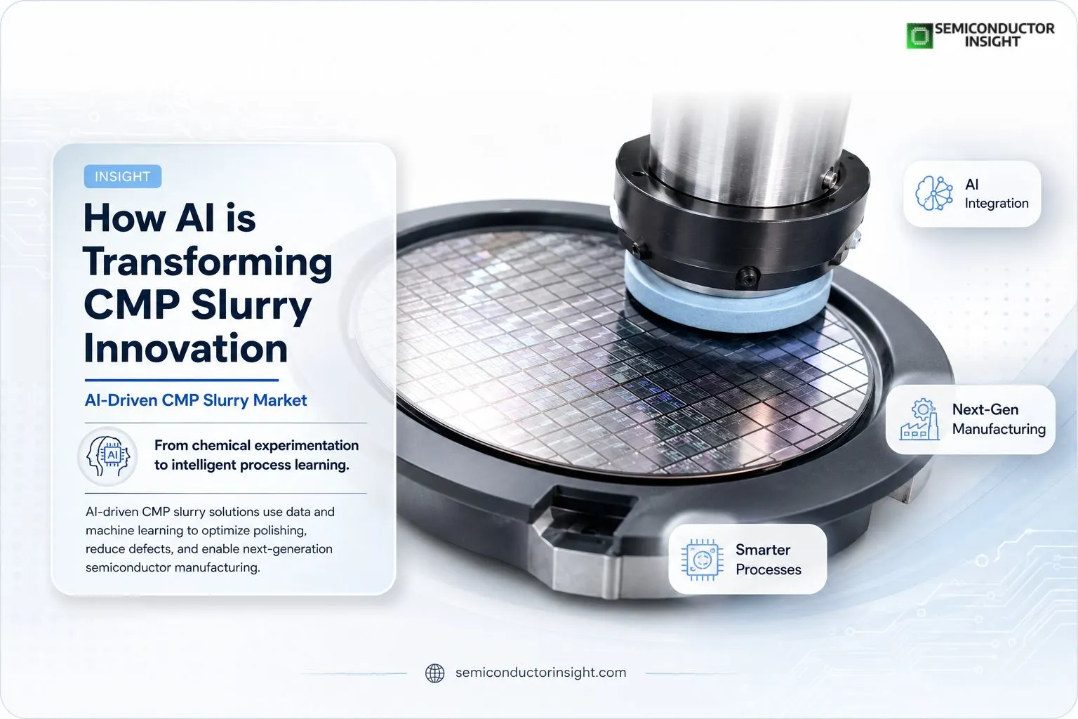
Artificial intelligence is no longer limited to chip design or manufacturing automation it is increasingly influencing the chemistry behind semiconductor fabrication. One of the most notable developments is AI-Driven CMP Slurry Market, where data analytics, machine learning, and process intelligence are being integrated into Chemical Mechanical Planarization (CMP) slurry development and optimization.
As semiconductor manufacturers transition toward 3 nm, 2 nm, and gate-all-around transistor architectures, maintaining atomic-level surface uniformity has become more demanding than ever. AI-driven slurry optimization enables manufacturers to predict polishing behavior, reduce defect formation, and improve wafer consistency without relying solely on traditional trial-and-error methods. The result is a smarter manufacturing ecosystem capable of delivering higher yields while supporting increasingly complex semiconductor devices.
From Laboratory Chemistry to Intelligent Process Learning
- Traditional CMP slurry development often required months of material testing across hundreds of polishing experiments.
- AI has significantly shortened this cycle by analyzing historical polishing datasets, wafer inspection images, pad wear characteristics, and process parameters simultaneously.
- Instead of optimizing only abrasive particle size or chemical concentration independently, AI models evaluate thousands of parameter combinations to recommend slurry formulations tailored for specific materials such as silicon carbide, cobalt, tungsten, copper, and dielectric films.
- Several semiconductor manufacturers are now integrating digital twins with CMP process control, allowing virtual testing before physical implementation.
- This approach accelerates material qualification while minimizing production interruptions.
Patent Landscape: Endpoint Detection at the Heart of CMP IP
Patent records show that endpoint detection is one of the most heavily litigated areas in chemical mechanical planarization (CMP) intellectual property.
A snapshot of granted U.S. patents behind today’s sensor-driven endpoint systems effectively the paper trail supporting many “AI-driven” claims includes: around US 5,321,304, which covers friction and motor-current-based endpoint detection tied to the resulting semiconductor device; approx. US 6,383,058, which introduces adaptive endpoint detection for CMP processes; approx. US 6,794,285, focused on silicone-surfactant CMP slurry formulations and their manufacturing methods; and around US 6,908,374, which details an optical, belt-based CMP endpoint detection system.
Numbers That Reflect the Growing Manufacturing Complexity
Several industry developments highlight why AI-driven CMP innovation is becoming strategically important.
- Modern semiconductor fabs process tens of thousands of 300 mm wafers every month, with each wafer passing through multiple CMP stages before completion.
- A single advanced logic chip may require 20 to 30 separate CMP operations throughout front-end manufacturing.
- Advanced AI processors now integrate tens of billions of transistors, demanding exceptionally smooth wafer surfaces to maintain electrical performance.
- Extreme Ultraviolet lithography systems support manufacturing resolutions below 20 nanometers, increasing dependence on highly controlled planarization processes.
- Today’s leading HBM memory stacks contain 12 to 16 vertically connected DRAM layers, requiring highly uniform polishing across multiple fabrication steps.
Where AI Meets Real-Time Wafer Intelligence
One of the most significant shifts involves connecting CMP equipment with factory-wide analytics platforms. Instead of detecting polishing issues after inspection, AI systems analyze vibration signals, slurry flow behavior, polishing pressure, motor current, endpoint detection, and optical measurements while polishing is taking place.
Machine learning algorithms continuously compare live production data with historical manufacturing records, enabling early identification of abnormal polishing conditions. This predictive capability helps reduce wafer scrap while improving process repeatability across high-volume manufacturing facilities.
Companies involved in semiconductor manufacturing equipment have also expanded AI-based predictive maintenance solutions, allowing polishing tools to maintain stable performance throughout longer production cycles.
The Rise of Digital Materials Development
AI is changing not only semiconductor manufacturing but also material innovation itself. Researchers now use generative AI and high-performance computing to simulate new abrasive particle structures, additive chemistries, oxidizers, corrosion inhibitors, and dispersants before laboratory synthesis begins.
Instead of evaluating hundreds of physical formulations, virtual screening identifies the most promising candidates within days. This shortens development timelines while reducing chemical waste and research costs. Several university research laboratories are combining AI with molecular simulations to better understand particle interactions during polishing, opening new opportunities for customized slurry design for future semiconductor materials.
To Stay Tuned with More meaningful and In-Depth Insights, Do Visit here: https://semiconductorinsight.com/report/ai-driven-cmp-slurry-market/
Why Advanced Packaging Is Creating New CMP Opportunities?
AI computing platforms increasingly rely on chiplets, heterogeneous integration, and advanced packaging technologies rather than larger monolithic chips. These packaging approaches introduce additional wafer bonding, redistribution layers, through-silicon vias, and hybrid bonding processes all of which require extremely precise planarization.
- For example, advanced packaging facilities supporting AI processors often perform multiple polishing cycles to prepare bonding surfaces with nanometer-scale flatness. AI-assisted slurry optimization improves surface quality while reducing defect density during these increasingly sophisticated manufacturing steps.
As demand grows for AI servers, automotive processors, high-bandwidth memory, and edge AI devices, intelligent CMP slurry technologies are becoming an important part of semiconductor production strategies rather than simply an

Comments (0)