EUV vs. High-NA EUV in ASML market Complete Technology Analysis
The semiconductor industry often celebrates breakthrough processors and AI accelerators, yet the technology enabling those innovations remains less visible. At the center of modern chip fabrication stands ASML, the sole commercial supplier of Extreme Ultraviolet (EUV) lithography systems. From advanced smartphones and AI servers to automotive processors, the world’s most advanced chips increasingly depend on ASML’s lithography ecosystem.
As semiconductor manufacturers pursue 2nm and smaller process technologies, lithography has become one of the most valuable stages in the fabrication process, transforming ASML market into a strategic pillar of global technology infrastructure.
Why High-NA EUV Is Becoming the Industry’s Most Watched Technology?
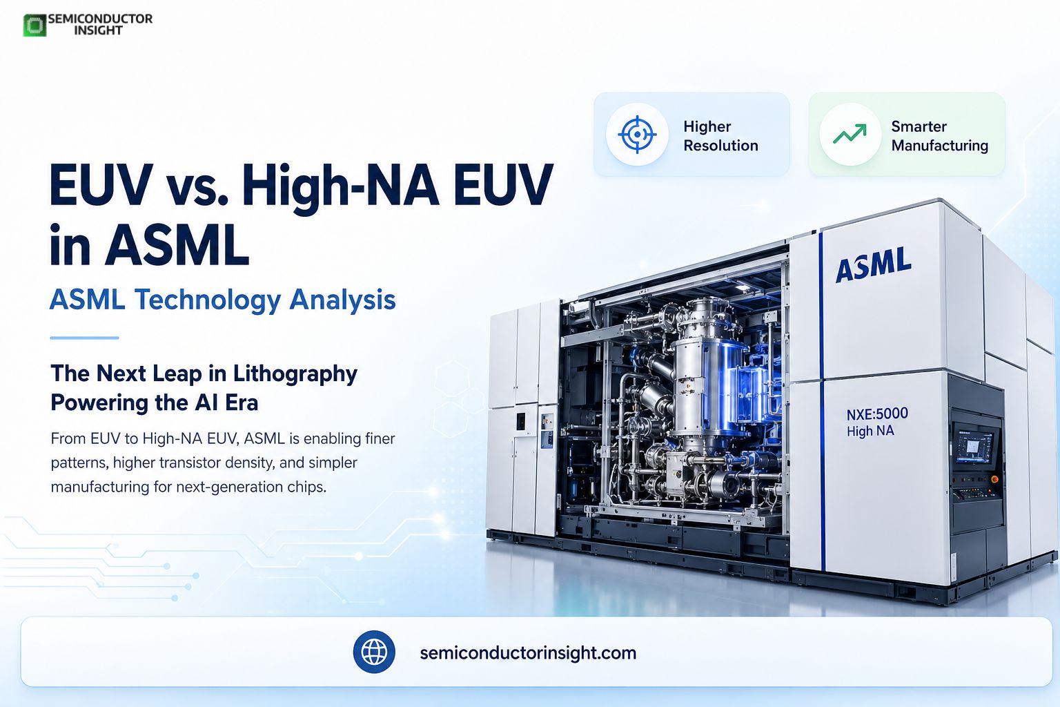
The transition from conventional EUV to High Numerical Aperture (High-NA) EUV represents one of the biggest manufacturing shifts in decades.
A single High-NA EUV system weighs approximately 150 metric tons and contains more than 100,000 components assembled with nanometer-level precision. These systems are designed to print increasingly complex transistor architectures required for next-generation AI processors.
Recent deployments by leading chip manufacturers demonstrate how High-NA tools are moving from research environments into commercial semiconductor production strategies. The technology is expected to reduce manufacturing complexity while enabling improved transistor density for advanced logic devices.
AI Infrastructure Is Quietly Expanding the ASML Opportunity
- The rapid growth of artificial intelligence has created unprecedented demand for advanced semiconductor manufacturing capacity.
- Training large AI models requires powerful GPUs and custom accelerators fabricated using cutting-edge process nodes. Every new AI data center indirectly increases demand for advanced lithography equipment.
- For example, major cloud providers continue investing billions of dollars into AI infrastructure, creating a chain reaction across the semiconductor supply ecosystem.
- Foundries are expanding wafer capacity, and lithography equipment remains one of the most critical investments supporting this expansion.
The Photoresist Connection Often Overlooked by Investors
While EUV machines receive most industry attention, photoresist materials remain equally essential to successful lithography.
Photoresist Market Share Insight;
- ArF photoresists continue to account for a significant portion of global semiconductor lithography material consumption.
- EUV photoresist demand is growing rapidly as advanced-node production expands.
- Leading suppliers from Japan maintain a dominant position in high-performance semiconductor photoresist production.
- The increasing adoption of High-NA EUV is expected to drive demand for next-generation photoresist formulations capable of supporting finer pattern resolutions.
Without continual advances in photoresist chemistry, the full capabilities of EUV and High-NA systems cannot be realized, making material innovation a key component of the broader ASML market ecosystem.
The Billion-Dollar Supply Chain Hidden Inside One Lithography Tool
An EUV lithography system is among the most complex manufacturing machines ever commercialized.
Each system integrates advanced optics, ultra-high vacuum chambers, laser-produced plasma light sources, precision motion stages, and highly specialized metrology technologies.
Industry reports and public company disclosures indicate that advanced EUV platforms can command prices exceeding USD 200 million per unit, highlighting the extraordinary engineering value embedded within every installation.
This complexity has created an ecosystem involving hundreds of specialized suppliers spanning Europe, Asia, and North America.
How Geopolitics Is Reshaping Equipment Strategies?
Semiconductor manufacturing has become a national priority across multiple economies.
Governments are supporting domestic chip production through incentive programs, manufacturing investments, and technology initiatives. As new fabrication facilities emerge in regions such as the United States, Europe, Japan, and parts of Asia-Pacific, demand for advanced lithography infrastructure continues expanding.
The result is a more geographically diversified semiconductor production landscape that could generate additional opportunities for advanced equipment deployment over the coming decade.
To Stay Tuned with More meaningful and In-Depth Insights, Do Visit here: https://semiconductorinsight.com/report/ai-accelerator-chip-market-2/
From Moore’s Law to Manufacturing Intelligence
The future of semiconductor scaling is no longer determined solely by transistor counts. Success increasingly depends on manufacturing precision, ecosystem collaboration, advanced materials, and lithography innovation.
ASML’s position at the intersection of optics, software, precision engineering, and semiconductor production places the company at the center of the industry’s next chapter. As AI computing, advanced packaging, and next-generation processors continue evolving, ASML market is expected to remain one of the most influential segments shaping global semiconductor advancement.
Comments (0)