

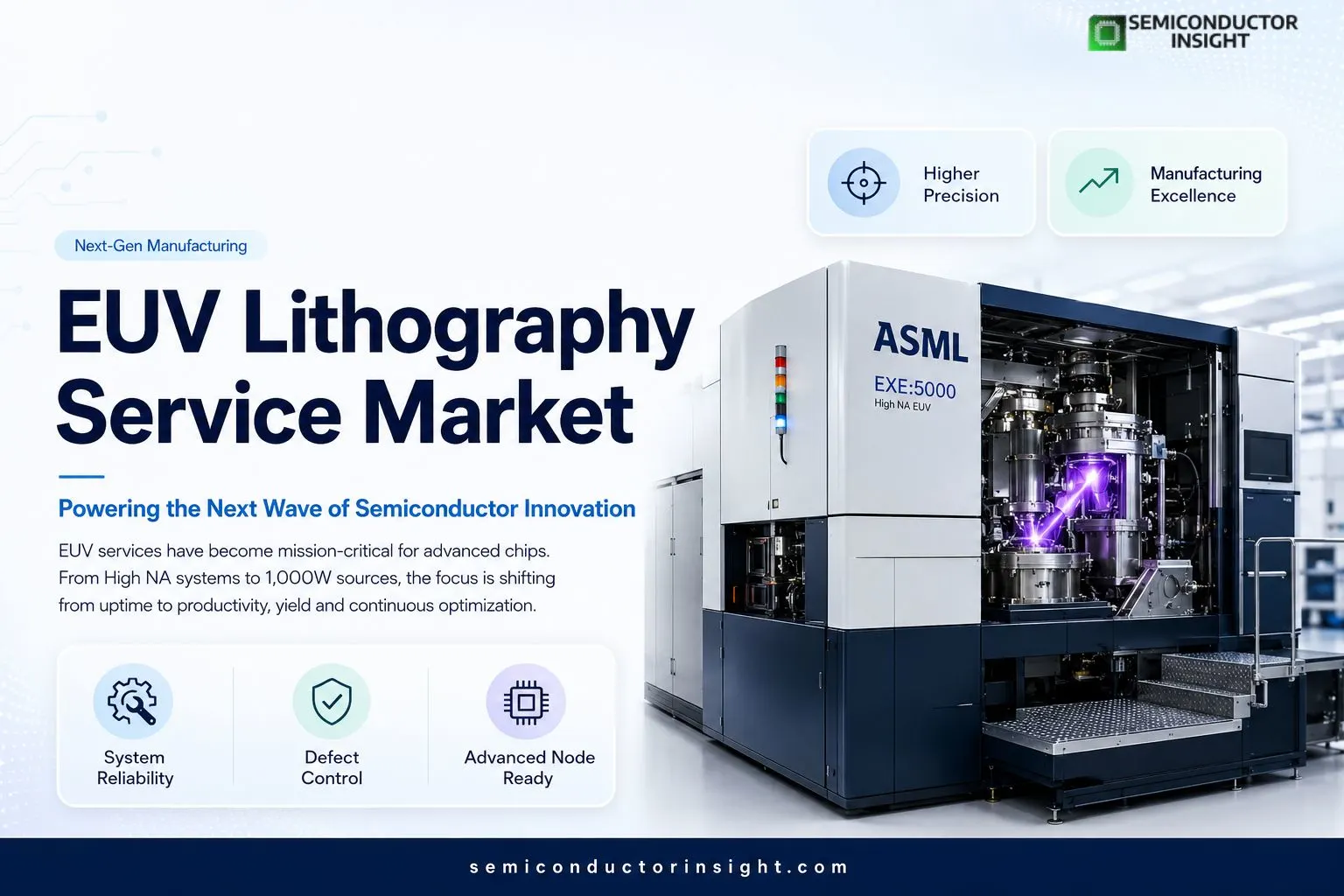
Conventional EUV vs. High NA EUV Lithography Services with Key Production Differences Explained
Extreme ultraviolet lithography is no longer an experimental technology sitting at the edge of semiconductor research. It has become a production-critical process for leading-edge chips, with service requirements extending well beyond the scanner itself.
Equipment installation, process qualification, computational lithography, overlay optimization, source maintenance, metrology coordination, mask handling and uptime support all form part of the wider EUV service ecosystem.
EUV uses 13.5 nanometer wavelength light, more than 14 times shorter than the 193 nanometer wavelength used by advanced ArF DUV systems. That shorter wavelength allows chipmakers to print extremely small features with fewer patterning steps.
For service providers, this means the commercial opportunity is increasingly tied to keeping extremely complex lithography equipment productive rather than simply supplying technical assistance.
A Machine Built Around Physics That Almost Feels Impossible
- A EUV scanner generates its light by firing laser pulses at microscopic molten tin droplets.
- ASML states that droplets of approximately 25 micrometers in diameter travel at around 70 meters per second, while the process can repeat up to 50,000 times per second. The resulting plasma produces the required 13.5 nanometer EUV radiation.
- The light cannot simply travel through conventional optical lenses because EUV radiation is absorbed by most materials. Instead, the system uses multilayer mirrors inside a vacuum environment. Each mirror contains more than 100 layers, while the optical surfaces are manufactured to extraordinary smoothness.
- This complexity creates a substantial requirement for specialized maintenance, calibration and process-control services.
48 Systems Shipped in One Year Changes the Service Equation
ASML’s 2025 annual report provides an important indicator of the installed EUV ecosystem. The company reported 535 total system sales in 2025, including 48 EUV lithography systems, alongside 279 DUV systems and 208 metrology and inspection systems. ASML also reported €4.7 billion in research and development expenditure during the year.
Every additional installed EUV system creates requirements for installation support, field service, spare components, software updates, calibration and productivity optimization.
That changes the service model from one-time equipment assistance toward a continuous lifecycle relationship with semiconductor fabs.
High NA Is Rewriting the Service Playbook
The most important technological transition now taking shape is High NA EUV. ASML’s EXE platform increases numerical aperture from 0.33 to 0.55, with the EXE:5000 designed around an 8 nanometer resolution. ASML says this can print features 1.7 times smaller in a single exposure and enable approximately 2.9 times higher transistor density compared with its NXE systems.
High NA therefore changes more than imaging. It introduces new optical configurations, faster stages, different process requirements and tighter control requirements.
For EUV service specialists, this creates a new technical environment:
Scanner installation → Optical calibration → Exposure optimization → Overlay control → Defect monitoring → Preventive maintenance → Production uptime
The service chain becomes increasingly interconnected with fab yield.
The 1,000 Watt Milestone Signals a Productivity Race
In April 2025, ASML demonstrated what it described as the first 1,000-watt EUV light source. Higher source power is important because productivity depends heavily on how efficiently enough EUV photons can be generated for wafer exposure.
This milestone matters to service markets because higher-power systems create additional demands around thermal management, source reliability, contamination control, component life and uptime monitoring.
The question for service organizations is therefore shifting from “Can the system operate?” toward “Can it operate continuously at the required productivity and yield?”
To find out more, feel free to browse our latest updated report: https://semiconductorinsight.com/report/extreme-ultraviolet-euv-lithography-service-market/
Why AI Chips Are Changing Lithography Support Requirements
The rapid expansion of AI computing is influencing the semiconductor manufacturing roadmap. ASML reported that demand for 0.33 NA EUV in 2025 was driven by advanced Logic and DRAM requirements associated with the build-out of AI infrastructure. The company also recognized revenue from four High NA EUV systems shipped to customer research and development facilities.
AI accelerators, high-bandwidth memory and advanced logic processors all depend on increasingly dense transistor structures. That puts greater emphasis on exposure accuracy, defect reduction and repeatability.
Lithography services consequently become closely linked with the production objectives of AI semiconductor manufacturers.
Pellicles and Defect Control Become Service-Critical
A tiny particle on a EUV mask can potentially become a repeating defect across multiple dies. EUV pellicles are therefore designed to protect reticles while allowing 13.5 nanometer radiation to pass through.
The engineering challenge is unusually demanding because the pellicle must remain extremely thin while surviving the thermal environment created during EUV exposure.
This opens additional service opportunities around mask inspection, pellicle qualification, and defect monitoring and exposure-process optimization.
From Equipment Support to Fab Productivity Management
- EUV lithography service market is increasingly evolving into a productivity-oriented ecosystem.
- Service teams are expected to understand not only mechanical or electrical maintenance but also imaging behavior, overlay, source performance, contamination, software control and wafer-level process results.
- High NA systems are reinforcing this transition. ASML says High NA EUV is designed to support future nodes beginning with 2 nanometer Logic, followed by memory applications at similar transistor densities.
The strongest service capabilities will therefore sit close to the manufacturing process itself. As EUV moves deeper into AI processors, advanced memory and next-generation logic, maintaining scanner uptime will remain important, but optimizing every exposure, every correction and every wafer will become an even more valuable part of the service equation.

Comments (0)