
AI for Waaf-Level Chip-Scale Package Design Market Insights
Global AI for Wafer-Level Chip-Scale Package Design market size was valued at USD 0.48 billion in 2025. The market moves from USD 0.48 billion in 2025 to USD 1.15 billion by 2034, exhibiting a CAGR of 9.3 % during the forecast period.
AI‑enabled wafer‑level chip‑scale package design combines machine‑learning models with traditional semiconductor layout tools to automate redistribution layer routing, die‑to‑substrate alignment and thermal‑stress prediction. By interpreting large datasets from prior silicon runs, the technology shortens design verification time while improving yield predictability.
The sector accelerates because semiconductor firms pursue higher I/O density and thinner form factors, while AI algorithms cut design cycles and reduce costly re‑spins. Recent activity underscores this trend; in April 2024, Synopsys announced a strategic partnership with TSMC to embed its AI design suite directly into TSMC’s advanced wafer‑level packaging flowlines. Other notable players such as Cadence Design Systems and Applied Materials are expanding their portfolios with AI‑driven simulation modules.
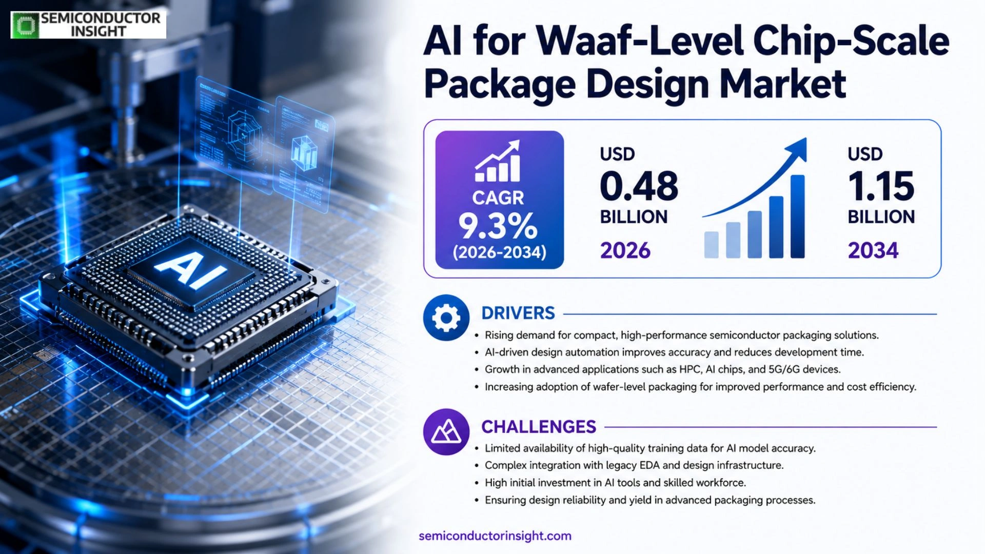
MARKET DRIVERS
AI‑Enabled Design Automation Gains Traction
The rollout of advanced neural networks for pattern recognition has lowered cycle times for wafer‑level chip‑scale package (CSP) layout by roughly 30 %, allowing manufacturers to meet aggressive time‑to‑market demands. This efficiency surge is being propelled by the convergence of high‑density interconnects and the need for tighter tolerances in emerging form factors.
Escalating Complexity of Heterogeneous Integration
As product portfolios incorporate mixed‑signal, RF, and power‑delivery modules within a single package, the combinatorial design space expands dramatically. AI algorithms now parse millions of layout permutations, surfacing viable configurations that human engineers would overlook. Companies that embed such capabilities report 15 % higher yield on first‑pass silicon.
➤ “AI is no longer a peripheral tool; it has become the core engine that transforms CSP design from art to science.”
Regulatory pressures for lower power consumption and smaller footprints reinforce this shift. By integrating AI early in the wafer‑level design flow, firms can pre‑emptively address thermal hotspots and signal‑integrity concerns, thereby reducing costly redesign cycles later in the product lifecycle.
MARKET CHALLENGES
Data Quality and Model Generalization
AI models rely on extensive historical design data, yet many fabs still operate with fragmented legacy archives. Inconsistent data labeling and limited representation of emerging materials make it difficult for algorithms to generalize across new process nodes, leading to prediction errors that erode confidence.
Other Challenges
Talent Scarcity
A shortage of engineers competent in both semiconductor physics and machine‑learning techniques hampers the pace at which companies can operationalize AI solutions, forcing reliance on external consultants and extending project timelines.
MARKET RESTRAINTS
High Capital Expenditure for Tool Integration
Implementing AI platforms requires substantial upfront investment in compute infrastructure, software licensing, and integration services. Mid‑size manufacturers, which comprise roughly 40 % of the CSP ecosystem, often lack the financial bandwidth to absorb these costs without jeopardizing other development projects.
Intellectual Property Concerns
The proprietary nature of design datasets raises questions about data ownership when leveraging third‑party AI providers. Companies wary of inadvertently exposing trade secrets may limit the depth of model training, thereby curtailing the technology’s full potential.
Regulatory scrutiny surrounding algorithmic decision‑making in safety‑critical applications adds another layer of compliance effort, slowing adoption among firms that must certify every design iteration.
MARKET OPPORTUNITIES
Cloud‑Based AI Ecosystems for CSP Design
Cloud platforms that bundle AI inference engines with scalable storage present a low‑entry barrier for smaller players. Subscription models enable firms to access cutting‑edge algorithms without the burden of maintaining on‑premise hardware, unlocking a 12 % annual growth in the segment of cloud‑enabled CSP services.
Collaboration Between AI Startups and Established Foundries
Strategic alliances are emerging where AI innovators supply tailor‑made models that complement established process flows. Such partnerships accelerate time‑to‑value, as foundries can quickly embed AI insights into their existing design‑for‑manufacturability checks, driving incremental revenue streams from value‑added services.
Finally, the rise of edge‑computing demands ultra‑compact, high‑performance packages. AI‑driven optimization of wafer‑level CSPs positions suppliers to capture a growing slice of the edge market, where design latency and power efficiency are paramount.
AI for Wafer-Level Chip-Scale Package Design Market Trends
Accelerating Design Cycles with AI‑Driven Automation
The integration of machine‑learning models into wafer‑level chip‑scale package design tools is compressing verification loops that previously spanned weeks. By ingesting historical layout data, the algorithms anticipate routing conflicts and thermal hotspots before physical prototypes are taped out, allowing engineers to resolve issues in a virtual environment. This shift not only shortens time‑to‑market for high‑density packages but also reduces the probability of costly design re‑spins, a factor that resonates strongly with manufacturers chasing slimmer form factors and higher I/O counts. The trend reflects a broader industry movement toward data‑centric engineering, where predictive analytics replace rule‑based heuristics.
Other Trends
Strategic Alliances Deepen AI Penetration
April 2024 marked a notable milestone when Synopsys entered a strategic partnership with TSMC to embed its AI design suite directly into TSMC’s advanced wafer‑level packaging flowlines. The collaboration supplies foundry customers with an end‑to‑end solution that fuses AI‑assisted layout optimization with TSMC’s process design kits, thereby creating a seamless pipeline from concept to silicon. Parallel moves by Cadence Design Systems and Applied Materials,both expanding portfolios with AI‑enhanced simulation modules,signal a competitive push to lock in ecosystem partnerships that can accelerate customer adoption and lock‑in revenue streams.
AI‑Enhanced Yield Predictability as a Competitive Lever
Yield models that combine deep‑learning inference with physical simulation are reshaping how manufacturers forecast production outcomes. By correlating subtle pattern variations in redistribution layer routing with observed defect densities, the AI layer produces probability maps that guide process engineers toward optimal parameter windows. This capability translates into more stable volume production, a critical advantage when product launch windows are tied to market cycles for emerging technologies such as 5G and automotive radar. Companies that embed these predictive tools into their design workflows are positioning themselves to offer differentiated services, potentially commanding premium pricing for guaranteed performance metrics.
COMPETITIVE LANDSCAPE
Key Industry Players
AI‑enabled wafer‑level chip‑scale package design: Competitive dynamics 2024‑2034
Synopsys dominates the AI‑driven packaging arena, principally because its recent AI design suite has been woven directly into TSMC’s advanced wafer‑level flowlines. The partnership, announced in April 2024, gives Synopsys a privileged channel to influence design standards across leading fabs, translating into a de‑facto platform for high‑density interconnect solutions. Cadence Design Systems follows closely, leveraging its long‑standing simulation heritage to embed machine‑learning accelerators within its PCB and IC layout tools. Both firms benefit from extensive IP portfolios and a global services network that allow rapid deployment of AI‑enhanced verification cycles, thereby reducing time‑to‑market for customers chasing thinner form factors and higher I/O counts.
Beyond the two market leaders, a cluster of specialists is shaping niche segments of the ecosystem. Applied Materials has expanded its AI‑based thermal‑stress prediction modules, giving customers a data‑rich view of yield risk early in the design phase. ANSYS and Altair contribute high‑fidelity simulation engines that now incorporate deep‑learning surrogates to accelerate electromagnetic and mechanical analyses. Mentor, part of Siemens EDA, offers AI‑assisted routing for redistribution layers, while NXP and IBM are piloting internal AI workflows to streamline silicon‑to‑package hand‑offs. Intel’s internal design teams are experimenting with generative AI for die‑to‑substrate alignment, and foundries such as GlobalFoundries and TSMC are opening APIs that let third‑party AI tools interface directly with process design kits. Collectively, these players diversify the value chain, creating opportunities for customers to select point solutions that align with specific performance or cost objectives.
List of Key AI for Wafer-Level Chip-Scale Package Design Companies Profiled
- Synopsys Inc.
- Cadence Design Systems, Inc.
- Applied Materials, Inc.
- ANSYS, Inc.
- Altair Engineering Inc.
- Mentor, a Siemens Business
- NXP Semiconductors NV
- IBM Corporation
- Intel Corporation
- GlobalFoundries Inc.
- TSMC (Taiwan Semiconductor Manufacturing Company)
- Lam Research Corporation
- Skywater Technology
Segment Analysis:
| Segment Category | Sub-Segments | Key Insights |
| By Type |
|
Design Automation
|
| By Application |
|
High‑Density I/O Packaging
|
| By End User |
|
Semiconductor Foundries
|
| By Technology Integration |
|
Machine‑Learning‑Assisted Layout
|
| By Design Phase |
|
Detailed Layout Synthesis
|
Regional Analysis: AI for Wafer-Level Chip-Scale Package Design Market
Regional fabs have embedded AI modules directly into their lithography and dicing workflows, creating a seamless loop between design intent and physical output. This integration shortens hand‑off delays, allowing design engineers to receive real‑time yield feedback and adjust package geometries before costly rework is required.
Governments and private conglomerates allocate a disproportionate share of their semiconductor R&D budgets toward AI‑based layout optimization, recognizing that marginal gains in package density yield outsized revenue lifts for high‑end devices.
Universities in the region have spun off joint programs that blend micro‑electronics with machine‑learning curricula, supplying a pipeline of engineers capable of bridging algorithmic theory with silicon realities.
Trade accords and export‑control regimes in Asia‑Pacific are being recalibrated to accommodate AI‑enabled design tools, granting firms clearer pathways for cross‑border technology transfer while preserving strategic IP.
North America
North America continues to leverage its deep pool of AI research talent to develop sophisticated predictive models for wafer‑level packaging. While domestic fabs lack the sheer volume of Asia‑Pacific’s production lines, they compensate with higher average selling prices and a customer base that values bespoke performance tuning. Partnerships between leading universities and chip designers facilitate rapid prototyping of AI‑driven layout generators, which are then validated on niche manufacturing nodes. The regional emphasis on intellectual property protection encourages firms to retain core algorithms in‑house, fostering a differentiated service offering that can command premium margins.
Europe
European manufacturers are capitalizing on stringent quality standards to position AI‑assisted packaging as a compliance‑driven differentiator. Regulatory bodies across the EU are issuing guidelines that implicitly favor AI‑backed design verification, prompting vendors to embed these capabilities into their design‑for‑manufacturability workflows. Collaborative clusters in Germany and the Netherlands blend sensor‑fusion AI with thermal‑aware packaging, aiming to meet automotive and industrial IoT performance criteria. Although the market scale is modest, the higher price point for certified solutions sustains a viable niche for European players.
South America
In South America, emerging semiconductor fabs are beginning to adopt AI tools as a shortcut to bridge the technology gap with more established regions. Local governments are rolling out incentive schemes that subsidize AI‑software licences for startups focused on wafer‑level packaging. This early‑stage adoption is less about volume and more about establishing a knowledge base that can later be leveraged for export‑oriented manufacturing. The region’s strategic focus on training programs ensures that a new generation of engineers will be fluent in both AI methodologies and chip‑scale design principles.
Middle East & Africa
Middle East and African economies are still in the exploratory phase of AI‑enhanced chip packaging. Investment primarily flows through sovereign wealth funds that target technology incubators abroad, allowing regional firms to import expertise rather than develop it domestically. Nonetheless, pilot projects in UAE’s free‑zone tech parks are testing AI models for rapid design iteration, signaling an intention to move beyond proof‑of‑concept. If these initiatives mature, they could create a foothold for the region in specialized niche markets that value rapid time‑to‑market.
Report Scope
This market research report provides a comprehensive analysis of the AI for Wafer-Level Chip-Scale Package Design Market , covering the forecast period 2026–2034. It offers detailed insights into market dynamics, technological advancements, competitive landscape, and key trends shaping the industry.
Key focus areas of the report include:
- Market Overview: The report begins with an overview outlining its current market scenario, key growth indicators, and industry transformation drivers. It discusses macroeconomic factors, demand–supply balance, regulatory landscape, and the strategic role of semiconductors in powering advancements across industries such as automotive, telecommunications, consumer electronics, and industrial automation.
- Market Size & Forecast: Historical data and future projections for revenue, unit shipments, and market value across major regions and segments.
- Segmentation Analysis: Detailed breakdown by product type, technology, application, and end-user industry to identify high-growth segments and investment opportunities.
- Regional Insights: Insights into market performance across North America, Europe, Asia-Pacific, Latin America, and the Middle East & Africa, including country-level analysis where relevant.
- Competitive Landscape: Profiles of leading market participants, including their product offerings, R&D focus, manufacturing capacity, pricing strategies, and recent developments such as mergers, acquisitions, and partnerships.
- Technology Trends & Innovation: Assessment of emerging technologies, integration of AI/IoT, semiconductor design trends, fabrication techniques, and evolving industry standards.
- Market Drivers & Restraints: Evaluation of factors driving market growth along with challenges, supply chain constraints, regulatory issues, and market-entry barriers.
- Stakeholder Insights: Insights for component suppliers, OEMs, system integrators, investors, and policymakers regarding the evolving ecosystem and strategic opportunities.
Primary and secondary research methods are employed, including interviews with industry experts, data from verified sources, and real-time market intelligence to ensure the accuracy and reliability of the insights presented.
FREQUENTLY ASKED QUESTIONS:
What is the current market size of AI for Wafer-Level Chip-Scale Package Design Market?
-> AI for Wafer-Level Chip-Scale Package Design market moves from USD 0.48 billion in 2025 to USD 1.15 billion by 2034, exhibiting a CAGR of 9.3 %
Which key companies operate in AI for Wafer-Level Chip-Scale Package Design Market?
-> Key players include Axalta Coating Systems, AkzoNobel, BASF SE, PPG, Sherwin-Williams, and 3M, among others.
What are the key growth drivers?
-> Key growth drivers include railway infrastructure investments, urbanization, and demand for durable coatings.
Which region dominates the market?
-> Asia-Pacific is the fastest-growing region, while Europe remains a dominant market.
What are the emerging trends?
-> Emerging trends include bio-based coatings, smart coatings, and sustainable rail solutions.

Get Sample Report PDF for Exclusive Insights
Report Sample Includes
- Table of Contents
- List of Tables & Figures
- Charts, Research Methodology, and more...
 Download Sample Report PDF


