
Top Aerosol Deposition Process AD Film Market Trends across Advanced Electronic Materials
Rapid advancements in semiconductor manufacturing are continuously driving demand for innovative thin-film technologies capable of delivering precision, durability, and high electrical performance. Within this evolving landscape, the Aerosol Deposition Process (AD Film) Market has emerged as an important technology enabling the creation of dense ceramic and functional films at room temperature.
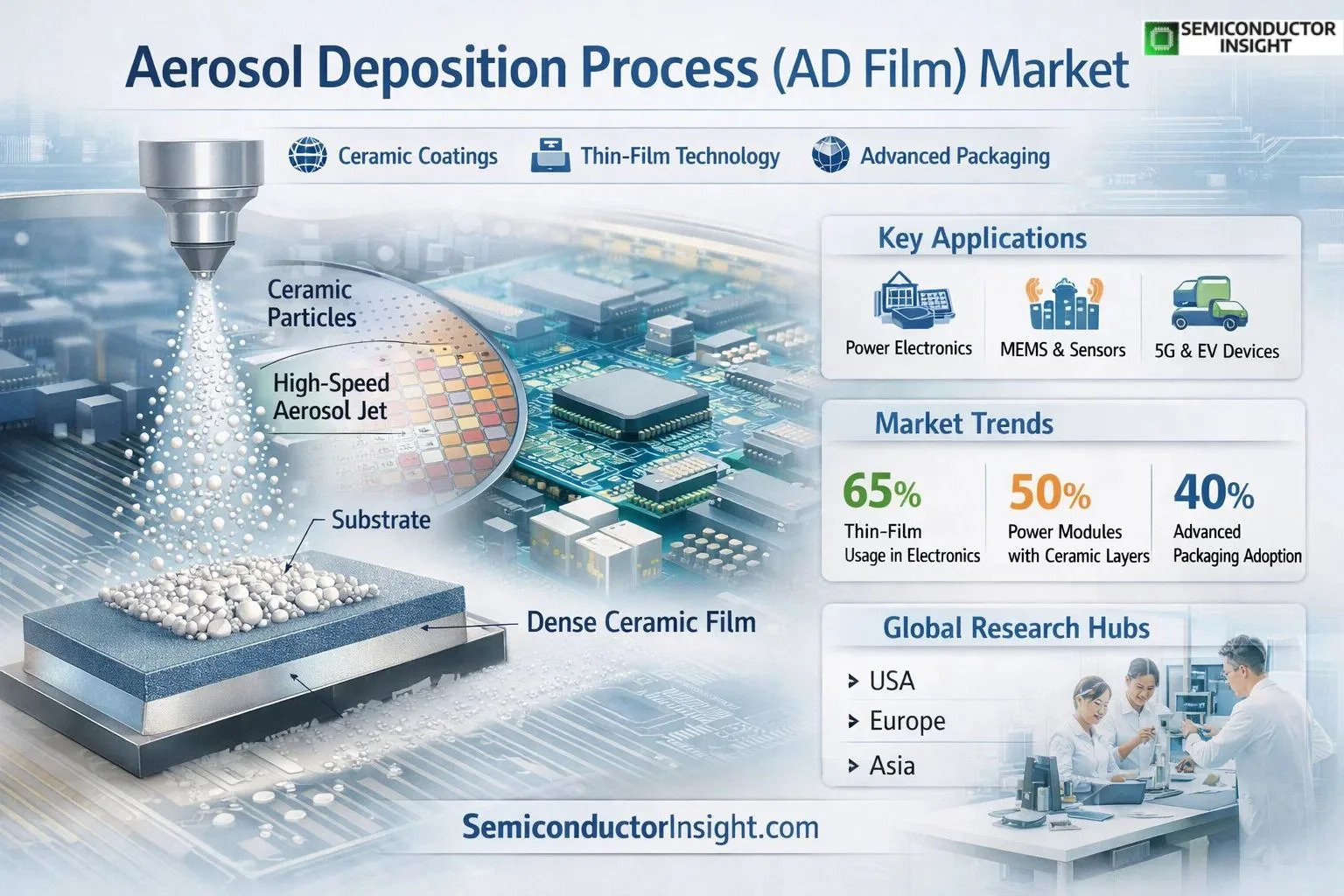
Aerosol deposition allows fine ceramic particles to be driven toward a substrate where they form dense layers through high-velocity impact, in contrast to conventional deposition methods that call for high temperatures or vacuum settings. This unique mechanism allows the production of extremely dense films without altering the properties of sensitive electronic components.
As semiconductor devices become smaller and more complex, the demand for advanced deposition techniques such as Aerosol Deposition, AD Film, Ceramic Films, and Semiconductors continues to expand across microelectronics and advanced materials research.
Precision Film Engineering for Modern Microelectronics
Thin-film technology plays a fundamental role in semiconductor device performance. Films are used for insulation layers, dielectric coatings, protective barriers, and conductive pathways in integrated circuits and electronic modules.
The aerosol deposition method enables film thickness ranging from a few micrometers to several tens of micrometers while maintaining strong adhesion to substrates such as silicon, glass, and metal surfaces. These characteristics make the technology particularly suitable for high-precision electronics where reliability is critical.
Industry research indicates that more than 65% of advanced electronic components rely on specialized thin-film coatings for electrical insulation and thermal stability. Technologies like aerosol deposition provide new pathways to manufacture these films efficiently while preserving material integrity.
Ceramic Coatings Powering Next-Generation Electronics
Ceramic materials such as alumina, zirconia, and titanium oxide are widely used in electronic coatings due to their excellent thermal resistance and electrical insulation properties. Aerosol deposition enables these materials to form dense layers without requiring sintering temperatures that could damage semiconductor substrates.
In power electronics, ceramic films play a crucial role in protecting components that operate under high voltage and extreme temperatures. Power modules used in electric vehicles, renewable energy converters, and industrial motor drives increasingly require durable protective coatings capable of withstanding thermal stress.
Studies show that nearly 50% of power electronic modules incorporate ceramic insulation layers, demonstrating the importance of reliable coating technologies within modern electronic systems.
Integration with Advanced Semiconductor Packaging
As chip architectures evolve, semiconductor packaging has become a critical stage in electronic device production. Advanced packaging techniques such as 3D stacking, system-in-package modules, and wafer-level integration require highly reliable insulating films and protective coatings.
Aerosol deposition technology offers advantages in this area because it can create thick and dense ceramic layers directly onto packaging substrates without exposing sensitive circuits to extreme processing conditions.
The adoption of advanced packaging technologies has increased significantly in recent years, with more than 40% of semiconductor devices now using multi-chip integration approaches. These complex structures often depend on robust thin-film coatings to maintain electrical isolation and long-term reliability.
Materials Innovation Driving Deposition Efficiency
Material engineering plays a major role in improving aerosol deposition performance. Researchers are continuously developing specialized ceramic powders with controlled particle size, morphology, and mechanical strength to enhance deposition quality.
Nanostructured powders and composite ceramic materials are gaining attention for their ability to produce films with improved mechanical properties and electrical performance. These materials can form coatings with minimal porosity while maintaining excellent adhesion to substrates.
Universities and semiconductor research laboratories are actively exploring hybrid ceramic coatings that combine insulating properties with thermal conductivity, helping electronic devices manage heat more effectively.
Industrial Equipment and Manufacturing Systems
The expansion of aerosol deposition technology has also led to the development of specialized manufacturing systems designed for high-precision film production. These systems typically include aerosol generation chambers, particle acceleration nozzles, and deposition chambers that allow controlled coating of substrates.
Automated deposition platforms are increasingly being integrated into semiconductor fabrication environments where process consistency and scalability are essential. Manufacturing facilities producing sensors, power modules, and advanced electronic components are adopting these systems to improve production efficiency.
Industrial automation and robotics are further enhancing the deposition process by enabling precise control over film thickness, deposition patterns, and substrate positioning.
You Can Go Through Our Latest Updated Insights Here: https://semiconductorinsight.com/report/aerosol-deposition-process-ad-film-market/
Research Momentum in Global Semiconductor Hubs
Research institutions and semiconductor technology centres across North America, Europe, and Asia are actively studying aerosol deposition applications. Collaborative projects between universities and electronics manufacturers are exploring new material systems and process improvements.
Countries investing heavily in semiconductor manufacturing infrastructure are particularly interested in deposition technologies that can support emerging electronic devices such as high-frequency communication chips, advanced sensors, and electric vehicle power modules.
More than 70% of semiconductor research laboratories worldwide are currently exploring advanced thin-film technologies to support next-generation electronics development. Aerosol deposition has become part of this broader effort to develop efficient and scalable coating processes.
Advancing Innovation in Electronic Applications
Beyond traditional semiconductor fabrication, aerosol deposition films are being used in several emerging electronic applications. These include microelectromechanical systems (MEMS), sensors, and energy storage components.
In sensor manufacturing, thin ceramic coatings help protect sensitive detection elements from environmental exposure while maintaining measurement accuracy. Similarly, electronic modules used in aerospace and industrial environments rely on robust coatings to withstand mechanical stress and temperature fluctuations.
As electronic devices become more compact and multifunctional, thin-film technologies capable of delivering reliability, insulation, and durability will remain critical to device performance.
Aerosol Deposition Process (AD Film) Market continues to gain attention as semiconductor manufacturers explore advanced material engineering solutions for next-generation electronics. With ongoing innovation in ceramic powders, deposition equipment, and semiconductor integration techniques, aerosol deposition is steadily positioning itself as a valuable technology within the evolving microelectronics ecosystem.

Comments (0)