
Acoustic Wave Filters Unlocking Precision in Modern Semiconductor Systems
In today’s hyper-connected semiconductor ecosystem, acoustic wave filters have quietly become one of the most critical components enabling seamless communication. These filters are embedded deep within RF front-end modules, ensuring that signals are transmitted with precision while eliminating unwanted interference.
As semiconductor devices evolve toward higher frequencies and multi-band operation, the importance of acoustic filtering has intensified. With over 45% of applications linked to consumer electronics, especially smartphones and wearable’s, these filters are now fundamental to chip-level performance optimization.
Decoding the Science of Noise Reduction and Signal Tuning
Acoustic wave filters operate using piezoelectric materials that convert electrical signals into mechanical waves and back again. This conversion allows them to selectively filter frequencies with exceptional accuracy.
Two dominant architectures define this space:
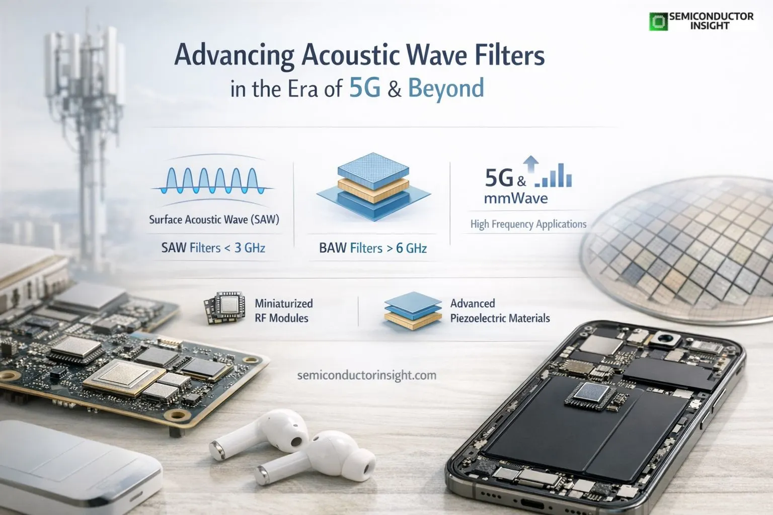
- Surface Acoustic Wave (SAW) filters, which dominate with nearly 49% share, are widely used in lower-frequency applications due to their cost efficiency and compact size.
- Bulk Acoustic Wave (BAW) filters, on the other hand, are designed for higher-frequency performance and are increasingly integrated into advanced 5G chipsets.
This dual-technology ecosystem ensures that semiconductor manufacturers can address both sub-6 GHz and emerging high-frequency spectrum needs.
Integration into RF Front-End Semiconductor Modules
Modern semiconductor chips have evolved beyond standalone processors into sophisticated communication hubs where acoustic wave filters serve as critical components in RF front-end modules. These filters enable multi-band signal handling, effective noise suppression in crowded frequency environments, and enhanced signal integrity for high-speed data transmission.
The rapid rollout of 5G infrastructure has dramatically increased filter requirements per smartphone, with devices now relying on dozens of filters to efficiently manage complex spectrum allocations. Acoustic wave filters command a dominant share of RF filter technologies, due to their compact design and exceptional performance in wireless applications.
Miniaturization and Semiconductor Design Evolution
As semiconductor nodes shrink and device architectures become more compact, acoustic wave filters are evolving in parallel. Engineers are focusing on:
- Ultra-miniaturized filter footprints
- Integration with system-in-package (SiP) modules
- Compatibility with advanced packaging technologies
Recent research has demonstrated acoustic filters operating at frequencies as high as 50 GHz, highlighting their potential for future 6G and millimeter-wave applications.
This shift toward high-frequency scalability is redefining how semiconductor companies approach RF design at the chip level.
Material Science Advancements in Piezoelectric Layers
Material innovation sets acoustic wave filters apart through performance gains. Quartz dominates with over 53% usage thanks to its proven stability and robust piezoelectric response.
Emerging alternatives like lithium niobate and scandium aluminum nitride are rapidly gaining ground, delivering higher electromechanical coupling, reduced signal loss at high frequencies, and superior thermal stability for crowded semiconductor environments. These breakthroughs prove essential as chips face extreme demands in AI systems, autonomous platforms, and next-generation communication networks.
Role in 5G and Emerging Semiconductor Architectures
The transition to 5G has dramatically elevated the importance of acoustic wave filters. Unlike earlier generations, 5G demands simultaneous support for multiple frequency bands, higher bandwidth with minimal signal distortion, and efficient filtering within crowded spectrum environments.
This shift has sparked surging demand for advanced acoustic filtering solutions integrated directly into semiconductor modules. Meanwhile, automotive electronics and IoT systems are emerging as key application areas where reliable signal processing proves essential.
Scaling Toward High Frequency Semiconductor Applications
One of the most exciting developments is the push toward high-frequency acoustic filters beyond 10 GHz. Traditionally, performance degradation limited their scalability, but recent innovations in thin-film technologies are overcoming these barriers.
New-generation filters now demonstrate:
- Improved bandwidth efficiency above 20 GHz
- Reduced insertion loss
- Enhanced rejection of unwanted signals
These capabilities are crucial for next-generation semiconductor applications, including mmWave communication and future 6G systems.
For more detailed info, be sure to review our newest exclusive related report: https://semiconductorinsight.com/report/rf-surface-acoustic-wave-filters-market/
Acoustic wave filter market is moving beyond being a passive component segment it is becoming a strategic enabler of semiconductor innovation. With the market projected to expand significantly from current levels, the focus is shifting toward integration, efficiency, and scalability.
As semiconductor ecosystems converge with AI, IoT, and advanced wireless technologies, acoustic wave filters will remain at the core of signal integrity and performance.
Their evolution reflects a broader trend in semiconductors: smaller components delivering higher precision in increasingly complex systems a transformation that defines the next era of electronics.

Comments (0)