
How 3D DRAM Stack HBM Packaging Market Is Reshaping Semiconductor Performance Standards?
The semiconductor industry is entering a new phase where computing power alone is no longer enough. Data movement speed, thermal management, and memory bandwidth have become equally important, especially in artificial intelligence systems. This transition is placing the 3D DRAM Stack High Bandwidth Memory (HBM) Packaging Market at the centre of global semiconductor discussions.
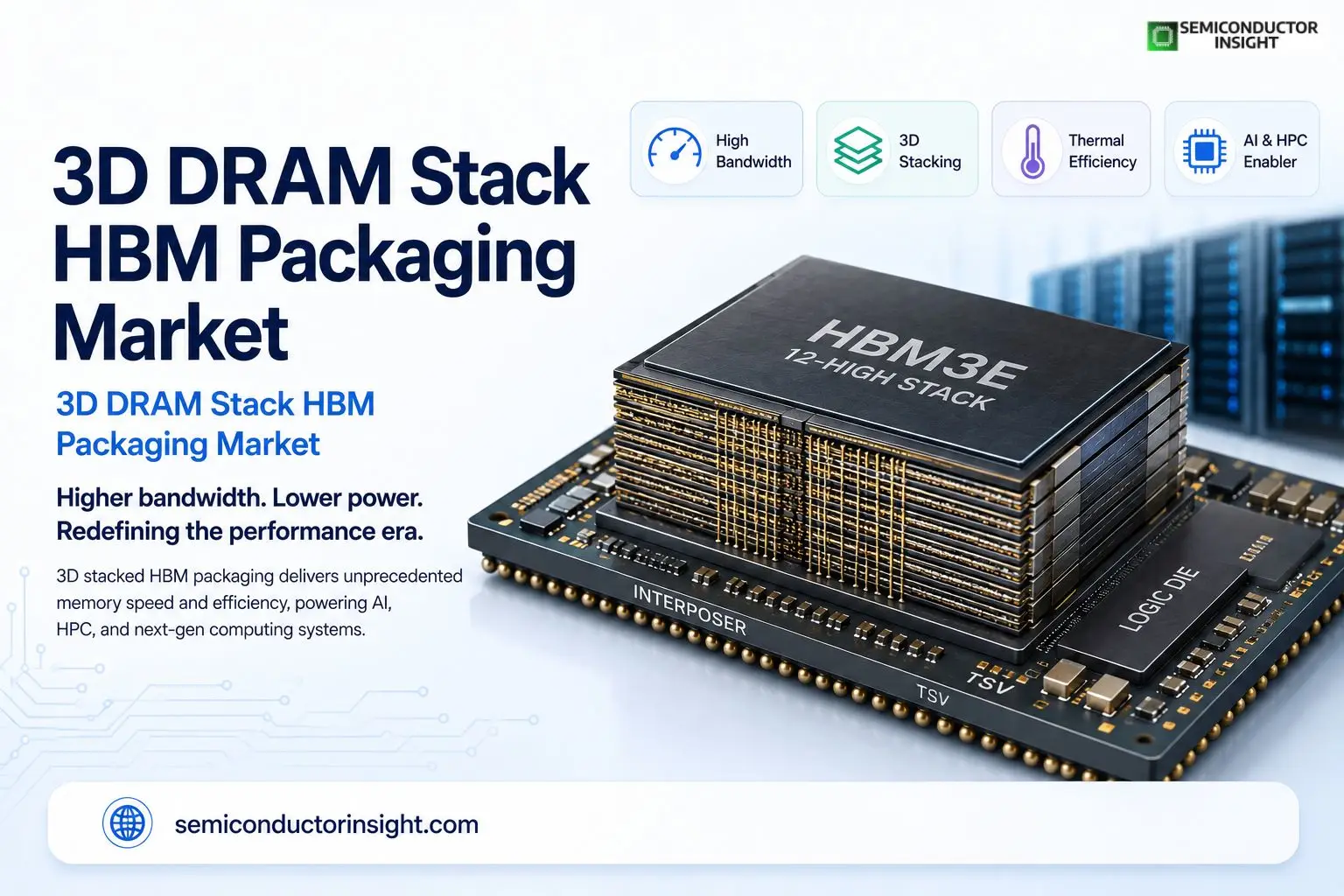
In contrast to standard DRAM layouts, HBM technology uses Through-Silicon Via (TSV) connections to stack several memory dies vertically. This architecture provides a substantial boost in bandwidth while consuming less power and requiring less board space. HBM packaging is becoming a must-have to retain performance efficiency. AI accelerators and powerful GPUs are processing huge datasets in parallel.
The recent surge in generative AI platforms, large language models, and AI training clusters has sharply increased demand for advanced memory packaging solutions. Semiconductor manufacturers are now competing not only on chip performance but also on packaging sophistication.
Stay connected for additional in-depth information right here: https://semiconductorinsight.com/report/3d-dram-stack-hbm-packaging-market/
AI Servers Are Consuming Memory at an Unprecedented Scale
- Modern AI data centres require enormous memory throughput to support model training and inference tasks. Advanced GPUs used in AI systems increasingly rely on HBM integration to manage high-speed data transfer between processors and memory stacks.
- Recent AI accelerators from companies such as NVIDIA and AMD are heavily dependent on HBM architectures. NVIDIA’s advanced AI GPUs integrate HBM technology to handle complex workloads involving billions of parameters.
According to technical disclosures presented during semiconductor conferences and corporate reports, some advanced AI processors now integrate memory bandwidth exceeding several terabytes per second. Traditional DRAM architectures struggle to achieve such levels efficiently, making HBM packaging increasingly indispensable.
- Taiwan-based foundries and outsourced semiconductor assembly providers are simultaneously expanding advanced packaging capacity to support rising AI demand. This includes large-scale investments in CoWoS and chip-on-wafer packaging technologies used alongside HBM integration.
The Packaging Layer Is Becoming More Valuable Than the Silicon Itself
Historically, semiconductor innovation focused primarily on transistor scaling. Today, packaging architecture is becoming equally strategic. The growing complexity of chiplet integration, thermal dissipation, and power delivery is changing how semiconductor value chains operate.
- HBM packaging requires highly specialised manufacturing capabilities involving TSV fabrication, wafer thinning, precision bonding, and advanced substrate engineering. Even minor alignment errors during stacking can impact signal integrity and yield rates.
- This has elevated the importance of packaging specialists within the semiconductor ecosystem. Companies that previously operated mainly as assembly providers are now playing a far larger technological role in AI hardware manufacturing.
Industry discussions during recent global semiconductor forums have increasingly highlighted packaging bottlenecks as one of the key limitations affecting AI hardware supply. Advanced packaging capacity shortages became visible throughout the recent AI server expansion cycle.
Heat Density Is Emerging as the Hidden Engineering Battle
One of the lesser-discussed aspects of HBM adoption is thermal intensity. Stacking memory dies vertically creates substantial heat concentration within compact areas. As AI processors consume more power, thermal engineering becomes critical for maintaining performance stability.
Semiconductor engineers are now exploring advanced cooling techniques, including liquid cooling systems, vapour chambers, and next-generation thermal interface materials. Data centre operators deploying AI clusters are also redesigning rack infrastructure to support higher thermal loads.
Several hyperscale cloud companies have already introduced liquid-cooled AI server deployments to handle dense GPU environments. This trend is indirectly accelerating innovation within the HBM packaging ecosystem because thermal efficiency directly impacts memory reliability and lifespan.
Semiconductor Geopolitics Is Influencing Memory Packaging Expansion
- The global semiconductor landscape is increasingly shaped by geopolitical priorities and supply chain localisation efforts. Governments across the United States, Japan, South Korea, Taiwan, and Europe are investing heavily in semiconductor infrastructure, including advanced packaging capabilities.
- The U.S. CHIPS and Science Act allocated billions of dollars toward semiconductor manufacturing and research initiatives, with advanced packaging identified as a strategic priority area. Japan has also strengthened collaboration with semiconductor firms to reinforce supply chain resilience for advanced memory technologies.
- South Korean memory manufacturers continue expanding HBM production as AI-driven demand accelerates. The competition surrounding HBM4 and next-generation memory standards is now becoming part of broader national semiconductor strategies.
Smaller Devices Are Demanding Bigger Performance
Beyond AI servers, HBM integration is beginning to influence automotive systems, high-performance gaming, defence electronics, and edge AI devices. Autonomous driving platforms processing real-time sensor data require high-speed memory performance while operating within compact hardware environments.
Advanced gaming GPUs are similarly benefiting from HBM architectures capable of supporting ultra-high-resolution rendering and AI-enhanced graphics processing. In aerospace and defence sectors, high-bandwidth memory is supporting radar processing, surveillance analytics, and advanced simulation systems.
This expanding application range demonstrates how advanced packaging is no longer confined to niche supercomputing environments. Instead, it is gradually becoming foundational to next-generation electronic systems.
Key Semiconductor Industry Snapshot
3D DRAM Stack HBM Packaging Market is expanding rapidly due to accelerating AI infrastructure investments, rising demand for high-performance computing, and increased deployment of advanced GPUs in cloud data centres.
HBM technology enables significantly higher memory bandwidth through vertically stacked DRAM dies connected via TSV technology, supporting AI training workloads and high-speed processing environments. Governments and semiconductor manufacturers globally are increasing investments in advanced packaging ecosystems to strengthen supply chain resilience and AI hardware production capabilities.
Important Industry Data Points
- Some next-gen AI GPU architectures are utilising HBM memory bandwidths of more than 3TB/s.
- The US CHIPS and Science Act provides more than USD 50 billion in incentives linked to semiconductors to promote manufacturing and packaging activities.
- Modern HBM stacks can have 8 to 12 vertically stacked DRAM dies, depending on the architecture generation.
- AI server racks are consuming an increasing amount of power, and some next-generation systems in dense deployments are topping 100 kilowatts per rack.
- Semiconductor makers are advancing the development of HBM4 memory standards to meet future AI accelerator needs.

Comments (0)