
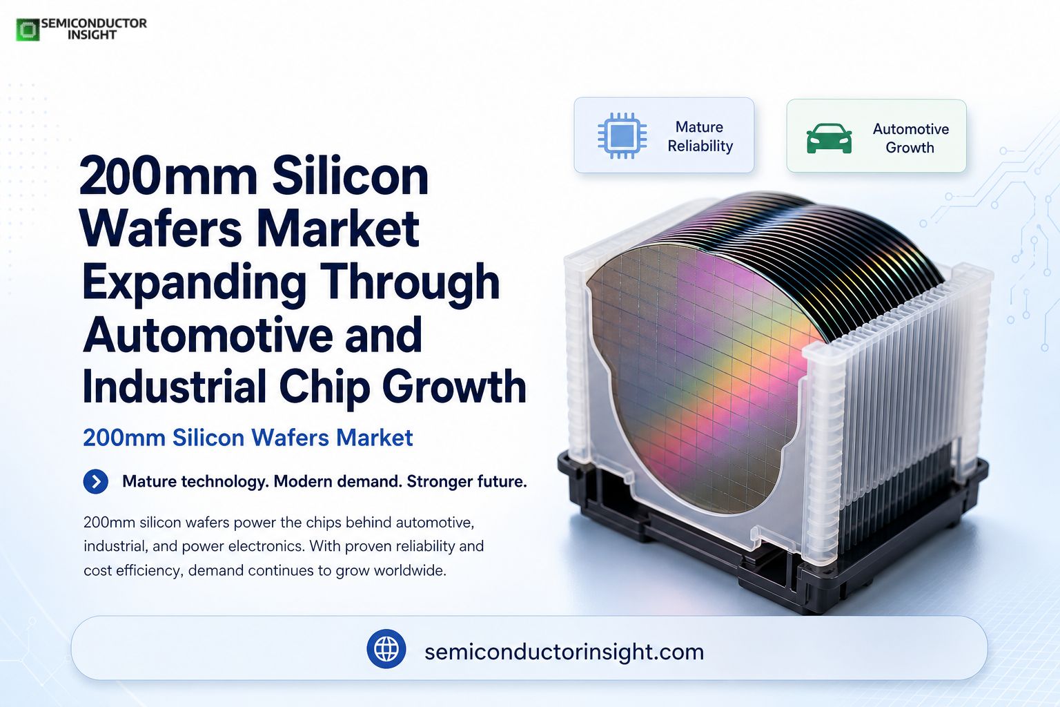
200mm Silicon Wafers Market Expanding Through Automotive and Industrial Chip Growth
While cutting-edge semiconductor headlines often revolve around 300mm wafers and sub-5 nm nodes, the 200mm silicon wafer remains deeply embedded in the global electronics backbone. These wafers, measuring 200 millimetres or 8 inches in diameter, are widely used in mature process nodes ranging from 90 nm to 350 nm. Such nodes are not obsolete; they are essential for analog ICs, power semiconductors, MEMS devices, and discrete components that power everyday electronics.
The durability of this segment is tied to its application base. Automotive electronics, industrial automation, and power management systems rely heavily on chips manufactured on 200mm wafers due to their robustness and cost efficiency. For instance, a typical automotive microcontroller built on a 200mm wafer process can operate reliably across temperature ranges from -40°C to 150°C, a requirement that advanced nodes are not always optimized for.
Fabrication Infrastructure and Global Installed Capacity
The installed base of 200mm fabrication facilities is substantial and continues to expand. According to industry data from organizations such as SEMI, there are over 200 operational 200mm fabs worldwide, with new capacity additions continuing each year. Monthly global production capacity has crossed 7 million wafers per month in recent cycles, reflecting sustained demand rather than decline.
A 200mm fab may be built or updated for far less money typically between $1 and $3 billion than 300mm fabs, which demand multi-billion-dollar investments surpassing $10-15 billion per plant. Both established producers and recent arrivals have been motivated to increase production because to this cost advantage, especially in areas emphasising semiconductor self-reliance.
A notable trend is the refurbishment of older fabs. Equipment originally installed in the early 2000s is being upgraded with modern automation and process control systems, extending operational life while improving yield rates.
You Can Go Through Our Latest Updated Insights Here: https://semiconductorinsight.com/report/200mm-silicon-wafers-market-size/
Device Ecosystem Anchored on 200mm Platforms
- The diversity of devices produced on 200mm wafers is one of the segment’s strongest foundations.
- Power devices such as MOSFETs and IGBTs dominate wafer utilization, especially with the rise of electric vehicles and renewable energy systems.
- A single electric vehicle can contain over 3,000 semiconductor chips, many of which are fabricated on 200mm wafers due to their suitability for power management.
- MEMS sensors represent another critical category. Accelerometers and gyroscopes used in smartphones, wearables, and automotive safety systems are predominantly produced on 200mm substrates.
- Annual global shipments of MEMS devices exceed 20 billion units, highlighting the scale of demand tied to this wafer size.
- Analog integrated circuits, which manage signal processing and voltage regulation, also rely heavily on 200mm wafers. These chips are foundational in industrial equipment, medical devices, and communication systems where precision and reliability outweigh the need for extreme miniaturization.
Equipment Lifecycle and Secondary Market Dynamics
One of the most unique aspects of the 200mm ecosystem is the thriving secondary equipment market. Since leading-edge fabs have transitioned to 300mm, a significant volume of 200mm equipment has been refurbished, resold, and redeployed. This circular equipment economy reduces capital expenditure and accelerates fab setup timelines.
Lithography tools, etchers, and deposition systems originally manufactured by companies like Applied Materials and Lam Research continue to operate efficiently after upgrades. In some cases, refurbished tools are sold at 40-60% lower cost compared to new systems, making them attractive for emerging fabs.
This reuse model also supports sustainability goals by extending equipment lifecycles and reducing the need for new manufacturing resources.
Material Specifications and Wafer Engineering Precision
- The production of 200mm silicon wafers involves highly controlled crystal growth and polishing processes. These wafers are typically manufactured using the Czochralski method, producing monocrystalline silicon ingots with precise dopant concentrations.
- Key specifications include wafer thickness of approximately 725 micrometres, surface flatness measured in nanometers, and defect densities kept below 0.1 defects per square centimeter for high-quality applications. Even minor deviations can impact yield, especially for analog and power devices where uniformity is critical.
- Polishing techniques such as chemical mechanical planarization ensure mirror-like surfaces required for photolithography. Each wafer undergoes multiple cleaning and inspection steps before entering fabrication lines, reflecting the precision demanded at every stage.
Supply Constraints and Lead Time Realities
Despite being a mature segment, the 200mm wafer market has experienced supply tightness in recent years. Lead times for certain wafer types have extended to 6-12 months, driven by strong demand from automotive and industrial sectors.
Unlike 300mm wafer production, which has seen aggressive capacity expansion, 200mm wafer manufacturing faces limitations due to fewer active suppliers and the high cost of building new crystal growth facilities. This imbalance has created a scenario where demand consistently outpaces incremental supply additions.
In response, wafer manufacturers are optimizing throughput and investing in incremental capacity upgrades rather than entirely new Greenfield projects.
Integration with Emerging Technologies
Interestingly, the 200mm platform is not isolated from innovation. It is increasingly being used for compound semiconductor integration, including silicon carbide (SiC) and gallium nitride (GaN) devices, which are essential for high-efficiency power electronics.
Some manufacturers are transitioning from 150mm to 200mm substrates for SiC production, improving economies of scale while maintaining performance advantages. This hybridization of mature wafer size with advanced materials reflects a unique evolution pathway that blends stability with innovation.
200mm silicon wafers market continues to operate as a foundational layer of the semiconductor ecosystem, quietly enabling billions of devices that define modern life while adapting to new technological demands through efficiency, reuse, and material innovation.

Comments (0)