
MARKET INSIGHTS
200mm silicon wafers market refers to the global ecosystem built around 8-inch silicon wafers used to manufacture semiconductor devices for power, analog, MEMS, microcontrollers, and automotive applications. These wafers sit at the center of mature-node chip production, where manufacturers still rely on proven, cost-efficient processes rather than chasing the smallest possible transistor size.
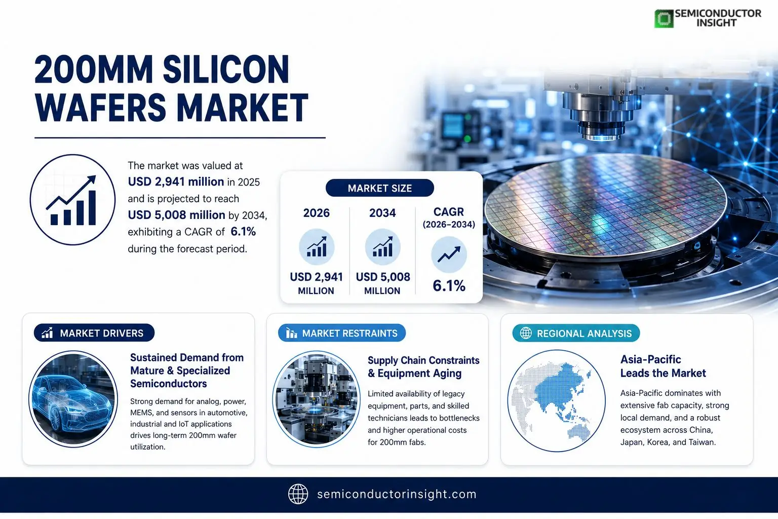
- The industry size was estimated at USD 2,941 million in 2025
- Forecast to surpass USD 5,008 million by 2034
- Demonstrating a CAGR of 6.1% during the forecast period
What keeps 200mm wafers important is their place in the semiconductor value chain. The industry is expanding 200mm fab capacity, with global capacity projected to exceed 7.7 million wafers per month by 2026, showing that this segment is far from legacy-only; it remains active and strategically important.
This market also benefits from its cost profile. Refurbished 200mm tools can cost 40% to 60% less than new equipment, which helps fabs extend the life of existing manufacturing lines and preserve a strong cost advantage.
Key Takeaways:
- Polished wafers lead the product mix, as they remain the most widely used base for mature-node semiconductor manufacturing and steady-volume chip production.
- Epitaxial wafers are gaining traction, supported by demand for power devices, analog ICs, and automotive-grade applications that need stronger electrical performance.
- Power/discrete devices and analog ICs stay at the center of demand, since 200mm lines are still the most practical fit for mature, cost-sensitive, and high-reliability semiconductor production.
MARKET DRIVERS
Sustained Demand from Mature and Specialized Semiconductor Applications
200mm silicon wafer Market is experiencing strong, steady demand primarily driven by the continued production of mature node semiconductors. These wafers are essential for a wide range of applications including analog chips, power semiconductors, micro-electromechanical systems (MEMS), and sensors. Unlike cutting-edge logic chips that require larger 300mm wafers, these devices are efficiently and cost-effectively manufactured on 200mm lines, ensuring the long-term viability of 200mm fab utilization.
Growth in Automotive and Industrial Electronics
The global expansion of automotive electrification, advanced driver-assistance systems (ADAS), and industrial automation is a significant driver. Each modern vehicle incorporates hundreds of chips, many of which, like power management ICs and various sensors, are produced on 200mm wafers. This demand is less cyclical than consumer electronics, providing a stable foundation for the market. The industrial Internet of Things (IIoT) further fuels need for robust, specialized semiconductors made on 200mm platforms.
➤ The global 200mm wafer fab capacity is projected to grow by over 15% in the next five years, highlighting the critical and enduring role of this segment.
Furthermore, the high cost of building new 300mm fabs for leading-edge nodes has led many semiconductor manufacturers to extend the lifecycle of their 200mm equipment. This cost-effective strategy maximizes return on existing capital investments and meets the persistent demand for legacy and specialty technologies.
MARKET CHALLENGES
Supply Chain Constraints for Legacy Equipment
A primary challenge for the 200mm wafer market is the scarcity and aging nature of manufacturing equipment. As equipment manufacturers have largely shifted focus to supporting 300mm and larger wafer sizes, sourcing replacement parts, refurbished tools, and qualified service technicians for 200mm fabrication lines has become increasingly difficult and expensive. This can lead to production bottlenecks and higher operational costs.
Other Challenges
Competition for Fab Capacity
The robust demand from various sectors creates intense competition for available 200mm fab capacity. This can lead to longer lead times and rising wafer prices, particularly for smaller fabless semiconductor companies that rely on foundry services.
Cost Pressure and Thin Margins
While 200mm manufacturing is cost-effective compared to new nodes, rising costs for raw materials, energy, and equipment maintenance exert significant pressure on profit margins for both wafer suppliers and foundries. Maintaining profitability requires highly efficient operations.
MARKET RESTRAINTS
Technological Limitations for Advanced Nodes
The fundamental restraint for 200mm silicon wafer Market is its incompatibility with the most advanced semiconductor process nodes (typically below 10nm). High-performance computing, smartphones, and advanced GPUs require the economies of scale and precision offered by 300mm wafers. This technological ceiling limits the market’s growth to mature and specialized segments, preventing expansion into the highest-value segments of the semiconductor industry.
Shifts in Capital Investment
The vast majority of new capital expenditure in the semiconductor industry is directed towards building and equipping new 300mm and 450mm wafer fabs. This long-term strategic focus on larger wafer sizes means that the 200mm segment receives minimal investment for new capacity creation, relying instead on optimizing existing infrastructure.
MARKET OPPORTUNITIES
Expansion in Compound Semiconductors and Advanced Packaging
Significant opportunities exist in the adoption of 200mm wafers for compound semiconductors like silicon carbide (SiC) and gallium nitride (GaN). These materials are crucial for high-power and high-frequency applications in electric vehicles and 5G infrastructure. The ability to utilize established 200mm manufacturing lines for these growth markets presents a major opportunity for wafer suppliers and foundries.
Modernization and Smart Manufacturing
The integration of Industry 4.0 technologies, including AI and IoT sensors, into 200mm fabs offers a substantial opportunity for operational improvement. Implementing smart manufacturing solutions can increase yield, reduce downtime, optimize maintenance schedules, and lower costs, thereby enhancing the competitiveness and profitability of existing 200mm production facilities.
200mm Silicon Wafers Market Trends
Strong Market Growth Fueled by Established Applications
The global 200mm Silicon Wafers market is demonstrating significant momentum, with its value projected to grow from US$ 3126 million in 2024 to US$ 4477 million by 2032, representing a Compound Annual Growth Rate (CAGR) of 6.9%. This sustained growth is primarily driven by the robust and continuous demand for semiconductors used in a wide range of mature and essential electronic components. These 8-inch wafers are fundamental to manufacturing devices in sectors such as automotive, industrial automation, and consumer electronics, where they are used for power/discrete devices, analog ICs, and sensors.
Other Trends
Persistent Demand Outpacing Supply
Despite the industry’s shift towards larger 300mm wafers for leading-edge logic and memory chips, demand for 200mm wafers remains exceptionally strong. This creates a distinct market dynamic where supply constraints are a key trend. The capital investment required for new 200mm fabrication facilities is often not justified compared to building state-of-the-art 300mm fabs, leading to a tight supply environment. This trend is supporting stable pricing and high utilization rates for existing 200mm wafer manufacturing capacity.
Consolidated Supplier Landscape and Geographic Shifts
The production of 200mm silicon wafers is highly concentrated, with the top 10 global players, including Shin-Etsu Chemical, SUMCO, and GlobalWafers, holding approximately 88% of the market share. This consolidation underscores the high barriers to entry and the specialized nature of wafer production. Geographically, Asia-Pacific dominates the market, both in terms of consumption and manufacturing capacity, driven by the presence of major semiconductor foundries and device manufacturers in countries like China, Japan, South Korea, and Taiwan. However, government initiatives in North America and Europe aimed at bolstering regional semiconductor supply chains are influencing investment and production trends.
COMPETITIVE LANDSCAPE
Key Industry Players
A Consolidated Market Dominated by Global Giants
200mm silicon wafer market is characterized by a high degree of consolidation, with the top players collectively commanding a significant majority of the market share. The competitive landscape is led by a few established global giants, with Shin-Etsu Chemical and SUMCO positioned as the dominant leaders. This market structure is driven by the substantial capital investment, advanced technological know-how, and long-standing customer relationships required for high-volume semiconductor substrate manufacturing. These leading companies are vertically integrated and benefit from economies of scale, allowing them to serve a diverse range of applications from power devices to image sensors. The market for 200mm wafers remains robust, supported by sustained demand from mature and specialized semiconductor segments that continue to rely on 200mm fabrication facilities.Beyond the market leaders, a number of other significant players occupy important niches, often with strong regional focuses. Companies such as Taiwan’s GlobalWafers and Germany’s Siltronic AG hold substantial global market shares and compete directly with the top players. Meanwhile, regional champions like South Korea’s SK Siltron, China’s National Silicon Industry Group (NSIG), and Taiwan’s Wafer Works Corporation are key suppliers within their respective geographical markets. The competitive dynamics are further influenced by specialized manufacturers producing advanced wafer types like Silicon-on-Insulator (SOI) wafers, exemplified by players like Soitec. This tier of companies faces the dual challenge of competing on cost with the largest suppliers while also differentiating their product offerings to cater to specific technical requirements.
List of Key 200mm Silicon Wafer Companies Profiled
- Shin-Etsu Chemical
- SUMCO
- GlobalWafers
- Siltronic AG
- SK Siltron
- FST Corporation
- Wafer Works Corporation
- Soitec
- National Silicon Industry Group (NSIG)
- Zhonghuan Advanced Semiconductor Materials
- Hangzhou Semiconductor Wafer
- GRINM Semiconductor Materials
- Shanghai Advanced Silicon Technology (AST)
- Zhejiang MTCN Technology
- Hebei Puxing Electronic Technology
Segment Analysis:
| Segment Category | Sub-Segments | Key Insights |
| By Type |
|
Polished Wafers remain the fundamental and most widely adopted product form, serving as the base substrate for a vast number of semiconductor devices due to their critical balance of surface quality, purity, and electrical properties. The Epitaxial Wafer segment is demonstrating significant growth momentum, driven by increasing demand for high-performance applications such as advanced power devices and specific analog ICs that require a grown crystalline layer to achieve superior electrical characteristics. While SOI wafers represent a more specialized, high-value niche, the annealed wafer segment also finds stable demand in applications requiring specific post-processing treatments to enhance material properties. |
| By Application |
|
The market is characterized by sustained and robust demand from the Power/Discrete Devices and Analog ICs segments, which together form the core application base for 200mm wafers. These segments benefit from the mature and cost-effective manufacturing ecosystem for 200mm fabs, making them ideal for a wide range of automotive, industrial, and consumer electronics. The Sensor application is also a significant growth area, particularly for image sensors used in automotive safety systems and consumer devices. Although mainstream high-performance logic has largely migrated to larger wafer diameters, the 200mm platform remains relevant for specific logic applications and microcontrollers. |
| By End User |
|
Integrated Device Manufacturers (IDMs) represent a cornerstone of demand, particularly for applications in the automotive and industrial sectors where they have deep expertise and established supply chains. Foundries are also major consumers, leveraging their flexible manufacturing capacity to serve a diverse set of fabless semiconductor companies requiring production for mature node technologies. While memory manufacturers primarily utilize larger wafers for volume production, they still maintain some 200mm capacity for specialized memory products, contributing to a steady, albeit more niche, demand stream. |
| By Doping Level |
|
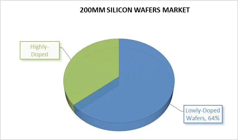
Lowly-doped wafers are the dominant choice for the majority of semiconductor fabrication processes, as they provide the high resistivity necessary for creating the active regions of transistors in logic, analog, and memory devices. The market for highly-doped wafers, while smaller, is critically important for specific applications such as power semiconductors and certain types of sensors where low resistivity substrates are required to minimize power loss or to serve as a highly conductive base layer. The choice between doping levels is fundamentally driven by the targeted device performance and electrical parameters. |
| By Supply Chain Role |
|
The market is primarily served by a concentrated group of leading merchant market suppliers who command a significant global market share and cater to the broad needs of foundries and IDMs. This structure creates a competitive landscape focused on consistent quality, high volume, and cost efficiency. However, a notable amount of captive production exists, particularly within large, vertically integrated IDMs who produce wafers for their own internal semiconductor fabrication to ensure supply chain security and tailor material specifications precisely to their proprietary processes. The interaction between these two supply models defines the overall market dynamics. |
By End User:
Regional Analysis: 200mm Silicon Wafers Market
Asia-Pacific
The region’s strength lies in its unparalleled concentration of 200mm fabrication facilities. Unlike other areas, Asia-Pacific benefits from a synergistic network of foundries, OSAT providers, and material suppliers, creating a highly efficient and resilient production environment for mature-node semiconductors that ensures steady supply and competitive pricing.
Local demand is a critical driver. The massive manufacturing base for automobiles, consumer gadgets, and industrial equipment within Asia-Pacific creates a powerful pull for the analog, power management, and display driver chips predominantly made on 200mm wafers, insulating the market from global demand fluctuations.
Decades of specialization have resulted in a deeply entrenched and highly skilled workforce alongside mature supply chains for legacy fabrication tools and wafer materials. This expertise allows for high yields and continuous process refinement, making 200mm production extremely cost-effective and reliable compared to newer regions.
While investment in leading-edge nodes continues, there is a parallel strategic focus on upgrading and expanding 200mm capacity to meet persistent demand. This includes initiatives to modernize equipment for enhanced efficiency and to develop specialized processes for emerging applications like sensors and MEMS, ensuring the region’s long-term dominance.
North America
North America maintains a significant, technologically advanced presence in the 200mm wafer market, though its focus differs from Asia-Pacific. The region is characterized by a strong base of integrated device manufacturers and specialty foundries that cater to high-reliability and specialized segments. Demand is particularly driven by the robust aerospace, defense, and industrial sectors, which require chips with long lifecycles and certifications that are ideally suited for mature 200mm processes. Additionally, the region’s vibrant ecosystem for innovation, including research institutions and fabless semiconductor companies, fuels demand for low-volume, high-mix production runs for prototyping and specialized analog, power, and RF chips. While the number of large-scale 200mm fabs is smaller than in Asia, the facilities that remain are often highly optimized for higher-margin, lesser-volume products, leveraging the region’s strength in design and intellectual property.
Europe
Europe’s 200mm silicon wafer market is defined by its strong foothold in the automotive and industrial semiconductor spaces. The region is home to major automotive OEMs and Tier-1 suppliers, creating substantial, consistent demand for the analog, power, and microcontroller units (MCUs) manufactured on 200mm lines. This demand is reinforced by stringent quality and safety standards prevalent in the European auto industry. Furthermore, Europe possesses a network of specialized fabs and R&D centers focused on areas like power semiconductors, sensors, and micro-electromechanical systems (MEMS), applications that are well-matched to 200mm wafer technology. The market dynamics are shaped by a focus on high-value, reliable components rather than high-volume commoditized parts, with strategic initiatives aimed at securing a sovereign supply of these critical chips for key industries.
South America
200mm silicon wafer Market in South America is relatively niche but shows potential for gradual growth, primarily driven by the increasing industrialization and digitalization of key economies like Brazil. Demand is largely import-dependent, servicing local manufacturing for consumer electronics, automotive assembly, and industrial equipment. The market dynamics are influenced by regional economic conditions and government policies aimed at fostering a domestic technology sector. While there is minimal local wafer production capacity, the region represents an important consumption market. Future growth is likely tied to broader economic stability and potential investments in developing a more robust local semiconductor ecosystem, though it remains a minor player compared to other global regions.
Middle East & Africa
The Middle East & Africa region represents an emerging market for 200mm silicon wafers, with dynamics centered on strategic economic diversification efforts, particularly in Gulf Cooperation Council (GCC) countries. Nations like Saudi Arabia and the UAE are making significant investments in technology hubs and semiconductor-related initiatives as part of long-term visions to reduce oil dependence. While local fabrication is currently limited, these investments are beginning to create demand for semiconductors, including those made on mature nodes. The broader African continent’s market is in its infancy, with demand linked to the growth of consumer electronics and telecommunications infrastructure. The region’s dynamics are characterized by high growth potential from a low base, driven by strategic national interests rather than an existing mature manufacturing base.
Report Scope
This market research report provides a comprehensive analysis of the Global 200mm Silicon Wafers Market, covering the forecast period 2025–2032. It offers detailed insights into market dynamics, technological advancements, competitive landscape, and key trends shaping the industry.
Key focus areas of the report include:
- Market Overview: The report begins with an overview outlining its current market scenario, key growth indicators, and industry transformation drivers. It discusses macroeconomic factors, demand–supply balance, regulatory landscape, and the strategic role of semiconductors in powering advancements across industries such as automotive, telecommunications, consumer electronics, and industrial automation.
- Market Size & Forecast: Historical data and future projections for revenue, unit shipments, and market value across major regions and segments.
- Segmentation Analysis: Detailed breakdown by product type, technology, application, and end-user industry to identify high-growth segments and investment opportunities.
- Regional Insights: Insights into market performance across North America, Europe, Asia-Pacific, Latin America, and the Middle East & Africa, including country-level analysis where relevant.
- Competitive Landscape: Profiles of leading market participants, including their product offerings, R&D focus, manufacturing capacity, pricing strategies, and recent developments such as mergers, acquisitions, and partnerships.
- Technology Trends & Innovation: Assessment of emerging technologies, integration of AI/IoT, semiconductor design trends, fabrication techniques, and evolving industry standards.
- Market Drivers & Restraints: Evaluation of factors driving market growth along with challenges, supply chain constraints, regulatory issues, and market-entry barriers.
- Stakeholder Insights: Insights for component suppliers, OEMs, system integrators, investors, and policymakers regarding the evolving ecosystem and strategic opportunities.
Primary and secondary research methods are employed, including interviews with industry experts, data from verified sources, and real-time market intelligence to ensure the accuracy and reliability of the insights presented.
FREQUENTLY ASKED QUESTIONS:
What is the current market size of the Global 200mm Silicon Wafers Market?
-> 200mm Silicon Wafers Market was valued at 2,941 million in 2025 and is projected to reach 5,008 million by 2034, exhibiting a CAGR of 6.1% during the forecast period.
Which key companies operate in the Global 200mm Silicon Wafers Market?
-> Key players include Shin-Etsu Chemical, SUMCO, GlobalWafers, SK Siltron, Siltronic AG, FST Corporation, National Silicon Industry Group (NSIG), Zhonghuan Advanced Semiconductor Materials, Wafer Works Corporation, and Zhejiang Jinruihong Technologies, among others. The global Top 10 players hold a share of about 88%.
What are the key growth drivers?
-> Key growth drivers include the robust growth of the global semiconductor manufacturing (wafer fabrication) market, which is projected to grow from USD 251.7 billion in 2023 to USD 506.5 billion by 2030, and the widespread use of 200mm wafers in applications such as Logic, Analog, Discrete devices, Micro-processors, Image Sensors, Power- and Optoelectronics, and IGBTs.
Which region dominates the market?
-> Asia is a dominant region in the market, with key countries including China, Japan, South Korea, and Southeast Asia.
What are the emerging trends?
-> Emerging trends include advancements in wafer types such as polished, annealed, epitaxial, and SOI wafers, and the integration of these wafers into a diverse range of semiconductor devices driven by increasing demand across various electronic applications.
Get Sample Report PDF for Exclusive Insights
Report Sample Includes
- Table of Contents
- List of Tables & Figures
- Charts, Research Methodology, and more...
 Download Sample Report PDF






