Market Insights
Global Wafer Metal Plating Service Market size was valued at USD 1.75 billion in 2025. The market is projected to grow from USD 1.92 billion in 2026 to USD 3.18 billion by 2034, exhibiting a CAGR of 6.8% during the forecast period.
Wafer metal plating services involve the deposition of thin metallic layers onto semiconductor wafers to enhance conductivity, corrosion resistance, and adhesion properties. These processes include electroplating, electroless plating, and other advanced techniques critical for semiconductor manufacturing, LED production, and microelectronics applications.
The market growth is driven by increasing demand for miniaturized electronic components, advancements in semiconductor fabrication technologies, and rising investments in IoT and AI-driven devices. Key players such as PacTech, JX Advanced Metals, and TANAKA are expanding their capabilities to meet the growing demand for high-precision wafer plating solutions.
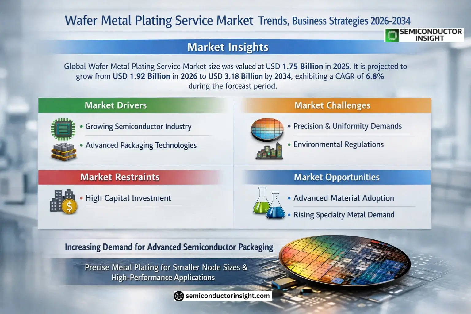
MARKET DRIVERS
Growing Semiconductor Industry Demand
Global Wafer Metal Plating Service Market is experiencing robust growth driven by the expanding semiconductor industry, which recorded a 8.5% year-over-year increase in 2023. As chip manufacturers push for smaller node sizes, advanced plating technologies are becoming essential for reliable interconnects and packaging solutions.
Emerging Advanced Packaging Technologies
Increased adoption of 2.5D and 3D IC packaging solutions is creating new demand for precision wafer plating services. The market for fan-out wafer-level packaging alone is projected to grow at a CAGR of 16% through 2028, requiring specialized plating processes for redistribution layers and through-silicon vias.
Automotive electrification trends are further accelerating demand, with semiconductor content in electric vehicles requiring 3-5 times more wafer plating services compared to conventional vehicles.
MARKET CHALLENGES
Precision and Uniformity Requirements
Meeting stringent thickness uniformity specifications (+/- 5% across 300mm wafers) presents significant technical challenges for plating service providers. The transition to <5nm nodes has reduced acceptable defect densities to fewer than 0.1 defects/cm², pushing plating process capabilities to their limits.
Other Challenges
Environmental Compliance Costs
Strict regulations on wastewater treatment and chemical usage in plating processes have increased operational costs by 15-25% for wafer metal plating service providers, particularly in North America and Europe.
MARKET RESTRAINTS
High Capital Investment Requirements
The average cost of setting up a 300mm wafer plating facility exceeds $50 million, creating significant barriers to market entry. Established players with existing cleanroom infrastructure and process expertise continue to dominate the Wafer Metal Plating Service Market.
MARKET OPPORTUNITIES
Advanced Material Adoption
Emerging plating materials like ruthenium and cobalt are gaining traction as alternatives to traditional copper plating, offering better performance at smaller nodes. The specialty metals segment in wafer plating is forecast to grow at 18% CAGR through 2027.
Wafer Metal Plating Service Market Trends
Increasing Demand for Advanced Semiconductor Packaging
Wafer Metal Plating Service Market is experiencing growth due to rising demand for advanced semiconductor packaging solutions. As chip manufacturers move toward smaller nanometer processes, precise metal plating becomes critical for interconnects and contact layers. Electroplating dominates the market segment as it offers superior conductivity and adhesion for high-performance applications.
Other Trends
Shift Toward Specialty Plating Solutions
Specialty plating techniques for wafer-level packaging are gaining traction, particularly for LED and MEMS applications. Companies are investing in chemical plating methods to achieve uniform thin-film deposition with tighter process control. This addresses the need for plating on sensitive substrates while maintaining yield rates.
Regional Market Developments
Asia-Pacific leads in Wafer Metal Plating Service adoption, driven by semiconductor manufacturing clusters in Taiwan, South Korea, and China. Key players are expanding production facilities to meet local demand, while North American providers focus on high-reliability plating for aerospace and defense applications. Environmental regulations in Europe are pushing innovations in wastewater treatment for plating processes.
Consolidation Among Service Providers
Strategic mergers between plating specialists and semiconductor equipment suppliers are reshaping the competitive landscape. Market leaders like PacTech and JCET Group are vertically integrating to offer end-to-end wafer processing solutions. This trend improves process consistency and reduces supply chain risks for foundry customers.
Technological Advancements in Plating Equipment
Automation and AI-driven process control systems are being adopted to enhance plating uniformity and reduce material waste. Next-generation plating tools incorporate real-time monitoring for thickness control, particularly for gold and nickel alloy deposition. These advancements help maintain quality standards in high-volume production environments.
COMPETITIVE LANDSCAPE
Key Industry Players
Global Wafer Metal Plating Service Market dominated by specialized semiconductor material providers
Global Wafer Metal Plating Service Market is characterized by the presence of both specialized semiconductor material providers and diversified electronics manufacturers. PacTech holds a significant market position due to its advanced packaging solutions, while JX Advanced Metals Corporation leads in high-purity metal plating technologies. The top five players collectively accounted for approximately XX% of global revenue in 2025, indicating a moderately concentrated market structure with established technology leaders.
Niche competitors like Sharretts Plating Company and Hillock Anodizing have gained traction through specialized electroplating solutions for advanced semiconductor applications. Emerging Asian players such as JCET Group are expanding their market presence through strategic partnerships and technology upgrades. The competitive landscape continues to evolve with increasing demand for advanced plating technologies in 3D IC packaging and wafer-level packaging applications.
List of Key Wafer Metal Plating Service Companies Profiled
- PacTech
- Sharretts Plating Company
- JX Advanced Metals
- Epson
- ProPlate
- Integrated Service
- TANAKA
- Hillock Anodizing
- JX Advanced Metals Corporation
- JCET Group
- Uyemura
- DuPont
- Evatec AG
- Lam Research
- Applied Materials
Segment Analysis:
| Segment Category | Sub-Segments | Key Insights |
| By Type |
|
Electroplating emerges as the dominant segment due to its widespread adoption in semiconductor manufacturing.
|
| By Application |
|
Semiconductor applications dominate the wafer plating market with critical requirements:
|
| By End User |
|
Foundries represent the largest consumer segment due to:
|
| By Metal Type |
|
Copper plating maintains leadership position with significant advantages:
|
| By Wafer Size |
|
300mm wafers dominate the plating services market with clear drivers:
|
Regional Analysis: Wafer Metal Plating Service Market
Asia-Pacific
Asian plating specialists lead in fan-out wafer-level packaging and 3D IC solutions, developing proprietary plating formulations for interconnects below 5μm pitch. Specialized through-silicon via (TSV) plating capabilities give regional providers technological edge.
Cluster-based service hubs near major semiconductor corridors optimize logistics costs. Shared infrastructure models and high-volume throughput capabilities enable wafer plating services at 15-20% lower costs than Western counterparts.
University-industry collaborations accelerate copper Electrochemical Deposition (ECD) advancements. Joint development programs with materials suppliers create tailored plating solutions for emerging memory and logic applications.
Proactive compliance with evolving REACH and RoHS directives positions regional players for long-term sustainability. Waste treatment facilities co-located with plating centers minimize environmental impact while maintaining cost structures.
North America
North America maintains wafer plating excellence through R&D intensive service providers supporting both IDMs and fabless companies. The market emphasizes cutting-edge solutions for compound semiconductor plating on GaAs and SiC wafers, crucial for 5G and electric vehicle applications. Defense and aerospace contracts sustain specialized gold and nickel plating services with stringent quality certifications. Regional players collaborate closely with equipment manufacturers to develop atomic-layer deposition compatible plating processes.
Europe
European wafer plating services focus on automotive-grade reliability and MEMS applications. Stringent environmental regulations drive innovation in cyanide-free gold plating and lead-free solder bump processes. The region benefits from strong materials science expertise, particularly in barrier layer plating for advanced packaging. Collaborative R&D initiatives between plating service providers and automotive semiconductor manufacturers ensure thermal cycling resilience.
Middle East & Africa
The emerging wafer plating market concentrates on backend services for consumer electronics supply chains. Strategic partnerships with Asian foundries bring technology transfer in basic copper and nickel plating services. Governments are investing in semiconductor infrastructure, creating opportunities for localized plating solutions. The region shows potential as a cost-competitive alternative for basic plating services with simpler technology nodes.
South America
Specialized plating services for analog and mixed-signal applications characterize the regional market. Local providers focus on niche markets including medical device packaging and industrial sensor plating. The proximity to North American markets creates opportunities for nearshoring certain plating processes. Workforce development programs aim to build technical capabilities in wafer-level plating for growing domestic semiconductor assembly demand.
Report Scope
This market research report provides a comprehensive analysis of the Wafer Metal Plating Service Market , covering the forecast period 2025–2034. It offers detailed insights into market dynamics, technological advancements, competitive landscape, and key trends shaping the industry.
Key focus areas of the report include:
- Market Overview: The report begins with an overview outlining its current market scenario, key growth indicators, and industry transformation drivers. It discusses macroeconomic factors, demand–supply balance, regulatory landscape, and the strategic role of semiconductors in powering advancements across industries such as automotive, telecommunications, consumer electronics, and industrial automation.
- Market Size & Forecast: Historical data and future projections for revenue, unit shipments, and market value across major regions and segments.
- Segmentation Analysis: Detailed breakdown by product type, technology, application, and end-user industry to identify high-growth segments and investment opportunities.
- Regional Insights: Insights into market performance across North America, Europe, Asia-Pacific, Latin America, and the Middle East & Africa, including country-level analysis where relevant.
- Competitive Landscape: Profiles of leading market participants, including their product offerings, R&D focus, manufacturing capacity, pricing strategies, and recent developments such as mergers, acquisitions, and partnerships.
- Technology Trends & Innovation: Assessment of emerging technologies, integration of AI/IoT, semiconductor design trends, fabrication techniques, and evolving industry standards.
- Market Drivers & Restraints: Evaluation of factors driving market growth along with challenges, supply chain constraints, regulatory issues, and market-entry barriers.
- Stakeholder Insights: Insights for component suppliers, OEMs, system integrators, investors, and policymakers regarding the evolving ecosystem and strategic opportunities.
Primary and secondary research methods are employed, including interviews with industry experts, data from verified sources, and real-time market intelligence to ensure the accuracy and reliability of the insights presented.
FREQUENTLY ASKED QUESTIONS:
What is the current market size of Wafer Metal Plating Service Market?
-> Wafer Metal Plating Service Market size was valued at USD 1.75 billion in 2025. The market is projected to grow from USD 1.92 billion in 2026 to USD 3.18 billion by 2034, exhibiting a CAGR of 6.8% during the forecast period.
Which key companies operate in Wafer Metal Plating Service Market?
-> Key players include PacTech, Sharretts Plating Company, JX Advanced Metals, Epson, ProPlate, Integrated Service, TANAKA, Hillock Anodizing, JX Advanced Metals Corporation, JCET Group, and Uyemura, among others.
What are the key growth drivers?
-> Key growth drivers include increasing demand for semiconductor devices, technological advancements in wafer plating, and expansion of the electronics industry.
Which region dominates the market?
-> Asia is the fastest-growing region, while North America remains a significant market.
What are the emerging trends?
-> Emerging trends include advanced plating techniques, eco-friendly plating solutions, and integration of automation in plating processes.
Get Sample Report PDF for Exclusive Insights
Report Sample Includes
- Table of Contents
- List of Tables & Figures
- Charts, Research Methodology, and more...


