Wafer ID Reader Market Insights
Wafer ID Reader market was valued at USD 35.94 million in 2025 and targets USD 105 million by 2034, reflecting a CAGR of 19.1 % over the period.
A Wafer ID Reader is a specialized identification device or software solution used for semiconductor manufacturing traceability and automated wafer handling control. Its core task is to reliably read wafer markings such as SEMI OCR, barcodes, Data Matrix,and QR Codes on highly reflective, low‑contrast or damaged surfaces, then feed the results to equipment control, sorting, lot merging, slot mapping and manufacturing execution systems. The typical technology stack combines dedicated optical paths, multi‑spectral or RGB illumination, automatic exposure control, flexible ROI settings and wafer‑oriented recognition algorithms; delivery formats range from single‑wafer fixed‑mount heads to batch cassette readers, software engines and integrated automation modules.
Market expansion stems from increasing automation in fabs, the need for tighter traceability on mature‑node and specialty processes, and growing localization efforts in key regions such as China and Korea. Suppliers that bundle optics, algorithms and SECS/GEM interfaces gain bargaining power because fab operators prefer turnkey solutions that minimise downtime. Competitive advantage therefore hinges on illumination geometry and code‑shift compensation rather than sheer camera resolution.
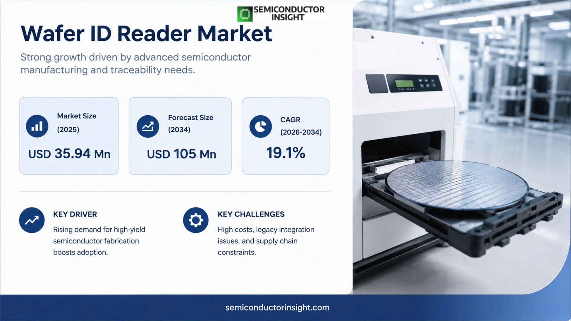
MARKET DRIVERS
Technological Convergence in Semiconductor Fabrication
Manufacturers are integrating high‑resolution imaging with real‑time data analytics, a shift that enhances traceability of each wafer from start‑up to final test. This convergence reduces scrap rates and shortens cycle time, making Wafer ID Reader market a pivotal element of modern fabs.
Demand for Inline Quality Assurance
Plants that embed identification readers directly on the production line can capture defect signatures at the moment they appear. By leveraging instant feedback, operators adjust process parameters before yield loss compounds, a capability that is increasingly mandated by OEM quality programs.
➤ “Embedding ID readers on critical process steps delivers a measurable lift in first‑pass yield, often exceeding 10 % in high‑mix environments.”
Beyond yield, the ability to link each wafer to a digital twin enables predictive maintenance of lithography tools, turning what was once a reactive expense into a strategic cost‑avoidance lever.
MARKET CHALLENGES
Integration Complexity with Legacy Equipment
Many fabs operate a mix of legacy and next‑generation tools. Retrofitting older scanners with modern ID readers demands custom interfaces, which inflate implementation budgets and extend commissioning timelines.
Other Challenges
Cost Sensitivity
Capital allocation committees often scrutinize any addition that does not present a clear, short‑term ROI, causing decision‑makers to postpone projects despite long‑term advantages.
Furthermore, the scarcity of skilled technicians who can calibrate and maintain these high‑precision devices introduces operational risk, especially in regions where training programs are limited.
MARKET RESTRAINTS
Regulatory Compliance Overhead
Compliance with industry standards such as IEC 61310 adds layers of documentation and validation. Companies that lack dedicated compliance teams find the bureaucratic overhead a deterrent to rapid adoption.
In addition, the need to certify each reader for clean‑room classifications raises both material costs and lead times, limiting the speed at which new deployments can roll out.
Finally, the fragmented nature of the supplier ecosystem means that buyers must juggle multiple contracts, increasing the administrative burden and occasionally leading to contract mismatches.
MARKET OPPORTUNITIES
AI‑Enhanced Inspection Platforms
Embedding machine‑learning models within Wafer ID Reader market ecosystem unlocks pattern‑recognition capabilities that surpass human visual inspection. Early adopters report up to a 12 % reduction in false‑positive defect calls, translating into faster throughput.
Another avenue lies in the migration toward Industry 4.0 standards, where interconnected readers feed data into centralized manufacturing execution systems. This data synergy supports real‑time optimization across the entire fab, creating a compelling value proposition for high‑volume producers.
Lastly, emerging niche applications,such as quantum‑dot wafer tracking and advanced packaging verification,present new revenue streams for vendors that can tailor their reader technology to ultra‑fine geometries.
Wafer ID Reader Market Trends
Integration of Wafer ID Readers into Automated Front‑End Systems
Wafer ID Reader market is moving from isolated, single‑wafer modules toward fully integrated identification subsystems that sit inside batch cassettes, sorters and front‑end automation equipment. Customers now evaluate a solution on the basis of how seamlessly it communicates with SECS/GEM, supports dual‑side reading and can be programmed to map slots without additional hardware. This shift raises the technical bar for suppliers, rewarding those that bundle optical design, algorithm libraries and communication stacks into a single package. For fabs, the payoff is a measurable reduction in manual interventions, tighter traceability and steadier throughput during high‑mix production runs.
Other Trends
Shift Toward Multi‑Band Illumination and Adaptive Exposure
Modern wafer surfaces present low‑contrast markings, film residues and occasional damage, circumstances that defeat conventional monochrome illumination. Vendors that incorporate RGB or multispectral LEDs together with automatic exposure control achieve read rates that stay above 99 % even on heavily etched 300 mm wafers. The ability to adjust ROI dynamically also means the same head can service both edge characters and dense Data Matrix codes, simplifying line design. As a result, equipment specifiers are prioritizing optical flexibility over raw sensor resolution, a nuance that reshapes R&D spend across the sector.
Regional Supply‑Chain Realignment and Competitive Positioning
Asia remains the primary engine of demand, yet the domestic substitution trend in China is prompting local firms to develop in‑house optics and algorithm suites. Korean and Taiwanese players continue to leverage strong export channels by embedding readers into high‑speed sorters, while European specialists focus on certified SEMI‑compliant interfaces for legacy equipment upgrades. This geographic diversification creates a market where switching costs are high,once a fab integrates a supplier’s communication protocol, re‑qualification becomes costly. Consequently, Wafer ID Reader market is evolving into a niche but sticky segment where deep integration capabilities and long‑term support outweigh simple price competition.
COMPETITIVE LANDSCAPE
Key Industry Players
Wafer ID Reader Market – Competitive Overview
The market is anchored by a handful of technology leaders whose breadth of optical design, algorithm libraries, and SECS/GEM integration give them a durable moat. Cognex Corporation leverages its deep OCR heritage and scales its VisionPro‑ID family across single‑wafer and batch‑cassette formats, capturing a sizable share of fab equipment OEM contracts in North America and Europe. IOSS GmbH, a German specialist, differentiates through multi‑spectral illumination modules that maintain read rates on low‑contrast, film‑covered wafer edges, making it the preferred supplier for high‑mix 200 mm lines. HST Vision in Japan complements these strengths with an emphasis on dual‑side, high‑throughput readers that are bundled into turnkey sorter platforms sold by major equipment makers. Together, these three firms dominate the upper‑mid tier of revenues, set de‑facto standards for interface compatibility, and steer the roadmap for next‑generation integrated automation solutions.
Beyond the incumbents, a vibrant cohort of niche innovators is expanding the functional envelope of wafer identification. Korea’s FAVIS and WACCO Technology deliver compact, cost‑effective readers that are increasingly embedded in locally produced sorters, while Chinese players such as HaiT Vision (Beijing) and Gazer Intelligent Control (Shanghai) focus on algorithmic adaptations for 8‑inch legacy lines and aggressive price positioning for domestic fabs. Taiwan’s FOXSEMICON and Germonic push integration depth by fusing ID reading with notch‑alignment and RFID tagging in front‑end automation modules. Southeast Asian outfits,including QES Group (Malaysia), R2D Automation (UK), RECIF Technologies (EU), EMU Technologies (UK), GL Automation (US), and Waftech (Malaysia),target specialty process nodes and offer software‑only engines that can be licensed to OEMs seeking to upgrade existing hardware. Their collective presence enriches the supplier ecosystem, forces the leaders to continuously improve performance, and gives fab customers bargaining leverage when negotiating long‑term service and upgrade contracts.
List of Key Wafer ID Reader Companies Profiled
- Cognex Corporation
- IOSS GmbH
- HST Vision Corporation
- FAVIS
- WACCO Technology Co., Ltd.
- HaiT Vision (Beijing) Technology Co., Ltd.
- Gazer Intelligent Control Sensor Technology (Shanghai) Co., Ltd.
- FOXSEMICON INTEGRATED TECHNOLOGY INC.
- QES Group Berhad
- R2D Automation
- RECIF Technologies
- EMU Technologies Ltd
- GL Automation, Inc.
- Germonic
- Waftech Sdn. Bhd.
Segment Analysis:
| Segment Category | Sub-Segments | Key Insights |
| By Type |
|
Single‑wafer fixed‑mount reader is regarded as the leading type because it delivers the most reliable performance on highly reflective wafer surfaces.
|
| By Application |
|
12‑inch high‑volume wafer lines dominate the application landscape as manufacturers pursue higher throughput and tighter traceability.
|
| By End User |
|
Wafer fabs are the primary end‑users because they anchor the entire traceability chain across the manufacturing workflow.
|
| By Functional Scope |
|
Read and Align/Map offers the greatest strategic advantage as it merges identification with precise wafer handling.
|
| By Product Form |
|
Integrated automation equipment is emerging as the preferred form because it consolidates multiple functions into a single footprint.
|
Regional Analysis: Wafer ID Reader Market
Fab densities in Taiwan and South Korea concentrate a majority of advanced‑node production, prompting equipment vendors to locate design centers nearby. Proximity shortens feedback loops, enabling rapid customization of ID readers to meet evolving process windows and allowing manufacturers to trial upgrades without extended lead times.
Recent geopolitical frictions have highlighted the need for diversified component sourcing. Asian firms are investing in local sensor fabrication and ASIC development, mitigating reliance on distant suppliers and ensuring a steadier flow of critical optics and illumination modules for wafer tracking solutions.
Regional authorities have introduced stricter traceability mandates for high‑value wafers, linking serial‑number capture to export licensing. Compliance pressures are translating into early adoption of robust ID readers, as manufacturers seek systems that can embed encrypted identifiers directly onto the wafer surface.
A surge in engineering talent graduating from top technical universities feeds a pipeline of specialists adept in optics, AI‑driven defect classification, and embedded firmware. This talent pool accelerates the rollout of next‑generation readers that combine hyperspectral imaging with edge‑compute capabilities.
North America
In North America, Wafer ID Reader market is shaped by a blend of legacy fabs and a growing focus on advanced packaging. The United States has leveraged federal R&D tax credits to encourage retrofitting of existing production lines with smarter identification hardware. While the overall volume of new wafer output lags behind Asia, the emphasis on security‑driven traceability,particularly for defense‑related semiconductor supplies,creates niche demand for readers that integrate cryptographic tagging. Partnerships between equipment manufacturers and cloud‑analytics firms are emerging, allowing customers to analyze identification data in real time and adjust process parameters on the fly.
Europe
European semiconductor clusters, especially in Germany and the Netherlands, prioritize precision engineering and sustainability. Industry consortia have advocated for ID readers that support low‑power operation while maintaining micron‑level accuracy, aligning with EU energy‑efficiency directives. Moreover, the region’s stringent data‑privacy regulations compel vendors to embed on‑device processing, limiting the transmission of wafer identifiers to external networks. These constraints have spurred a wave of boutique manufacturers offering modular reader platforms that can be tailored to specific fab environments, reinforcing Europe’s reputation for high‑quality, compliant solutions.
South America
South America’s involvement in Wafer ID Reader market remains modest, yet it is evolving as local governments promote semiconductor value‑addition to diversify economies traditionally reliant on raw‑material exports. Brazil’s recent investment in a pilot fab has generated interest in cost‑effective identification tools that can be deployed without extensive training. Vendors are responding with simplified reader kits coupled with remote‑support services, allowing smaller manufacturers to achieve traceability standards comparable to those in more mature markets.
Middle East & Africa
The Middle East & Africa region is at an early stage of adopting wafer identification technologies, largely driven by emerging investment zones in the United Arab Emirates and Egypt. These hubs aim to attract global semiconductor players by offering tax incentives and state‑of‑the‑art infrastructure. As a result, equipment suppliers are positioning modular, plug‑and‑play ID readers that can be quickly integrated into newly built fabs. Early adopters view the technology as a differentiator that signals compliance with international quality norms, positioning the region to capture a share of the market as production capacity expands.
Report Scope
This market research report provides a comprehensive analysis of the Wafer ID Reader Market , covering the forecast period 2026–2034. It offers detailed insights into market dynamics, technological advancements, competitive landscape, and key trends shaping the industry.
Key focus areas of the report include:
- Market Overview: The report begins with an overview outlining its current market scenario, key growth indicators, and industry transformation drivers. It discusses macroeconomic factors, demand–supply balance, regulatory landscape, and the strategic role of semiconductors in powering advancements across industries such as automotive, telecommunications, consumer electronics, and industrial automation.
- Market Size & Forecast: Historical data and future projections for revenue, unit shipments, and market value across major regions and segments.
- Segmentation Analysis: Detailed breakdown by product type, technology, application, and end-user industry to identify high-growth segments and investment opportunities.
- Regional Insights: Insights into market performance across North America, Europe, Asia-Pacific, Latin America, and the Middle East & Africa, including country-level analysis where relevant.
- Competitive Landscape: Profiles of leading market participants, including their product offerings, R&D focus, manufacturing capacity, pricing strategies, and recent developments such as mergers, acquisitions, and partnerships.
- Technology Trends & Innovation: Assessment of emerging technologies, integration of AI/IoT, semiconductor design trends, fabrication techniques, and evolving industry standards.
- Market Drivers & Restraints: Evaluation of factors driving market growth along with challenges, supply chain constraints, regulatory issues, and market-entry barriers.
- Stakeholder Insights: Insights for component suppliers, OEMs, system integrators, investors, and policymakers regarding the evolving ecosystem and strategic opportunities.
Primary and secondary research methods are employed, including interviews with industry experts, data from verified sources, and real-time market intelligence to ensure the accuracy and reliability of the insights presented.
FREQUENTLY ASKED QUESTIONS:
What is the current market size of Wafer ID Reader Market?
-> Wafer ID Reader market targets USD 105 million by 2034, reflecting a CAGR of 19.1 % over the period.
Which key companies operate in Wafer ID Reader Market?
-> Key players include Cognex Corporation (US), IOSS GmbH (EU), HST Vision Corporation (JP), FAVIS (KR), WACCO Technology Co., Ltd. (KR), HaiT Vision (Beijing) Technology Co., Ltd. (CN), Gazer Intelligent Control Sensor Technology (Shanghai) Co., Ltd. (CN), FOXSEMICON INTEGRATED TECHNOLOGY INC. (TW), QES Group Berhad (MY), R2D Automation (UK), RECIF Technologies (EU), EMU Technologies Ltd (UK), GL Automation, Inc. (US), Germonic (TW), Waftech Sdn. Bhd. (MY).
What are the key growth drivers?
-> Key growth drivers include rising demand for robust wafer traceability, increasing automation in semiconductor fabs, the need for dual‑side and batch wafer identification, and regional localization efforts,particularly in China, Korea and Taiwan,that spur investment in dedicated optical and algorithmic solutions.
Which region dominates the market?
-> Asia‑Pacific dominates Wafer ID Reader market, driven by the concentration of semiconductor manufacturing activities in China, Japan, South Korea and Taiwan.
What are the emerging trends?
-> Emerging trends include integration of Wafer ID Readers into batch cassette and front‑end automation equipment, AI‑enhanced recognition algorithms, multi‑spectral illumination designs, and tighter SECS/GEM communication interfaces for seamless fab‑level traceability.

Get Sample Report PDF for Exclusive Insights
Report Sample Includes
- Table of Contents
- List of Tables & Figures
- Charts, Research Methodology, and more...
 Download Sample Report PDF