Market Insights
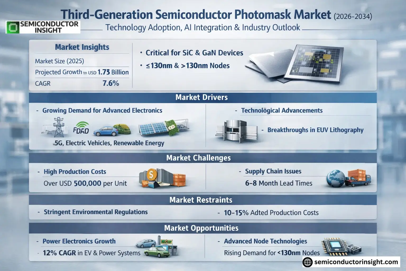
Global Third-Generation Semiconductor Photomask Market size was valued at USD 1.75 billion in 2025. The market is projected to grow from USD 1.92 billion in 2026 to USD 3.45 billion by 2034, exhibiting a CAGR of 7.6% during the forecast period.
Third-generation semiconductor photomasks are critical components used in the fabrication of advanced semiconductor devices, particularly those based on materials like silicon carbide (SiC) and gallium nitride (GaN). These photomasks enable precise patterning during lithography processes, ensuring high-performance electronic and optoelectronic applications. The technology supports both ≤130nm and >130nm node designs, catering to diverse industry requirements.
The market growth is driven by increasing demand for power electronics, RF devices, and LED applications, alongside advancements in electric vehicles and renewable energy systems. Key players such as Photronics, Toppan, and DNP dominate the market with extensive product portfolios and strategic collaborations aimed at enhancing production capabilities for next-generation semiconductor solutions.
MARKET DRIVERS
Growing Demand for Advanced Electronics
Third-Generation Semiconductor Photomask Market is experiencing significant growth driven by increasing demand for high-performance electronics. With applications in 5G technology, electric vehicles, and renewable energy systems, these advanced photomasks enable smaller, more efficient semiconductor devices. The market is projected to grow at a CAGR of 8.7% over the next five years.
Technological Advancements in Semiconductor Manufacturing
Breakthroughs in extreme ultraviolet (EUV) lithography have created new opportunities for Third-Generation Semiconductor Photomasks. These innovations allow for more precise patterning at nanometer scales, critical for next-generation chips. Leading manufacturers are investing over USD 2 billion annually in photomask R&D to maintain competitive advantage.
With the rise of IoT and AI applications, Third-Generation Semiconductor Photomasks are becoming essential components in the global supply chain for high-tech industries.
MARKET CHALLENGES
High Production Costs and Complexity
The manufacturing process for Third-Generation Semiconductor Photomasks requires ultrapure materials and specialized equipment, leading to production costs that can exceed USD 500,000 per unit. This creates significant barriers to entry for smaller players in the market.
Other Challenges
Supply Chain Disruptions
Global semiconductor shortages have created bottlenecks in photomask production, with lead times extending to 6-8 months for advanced designs. This impacts time-to-market for new semiconductor products.
Technical Limitations
As feature sizes shrink below 5nm, maintaining defect-free photomasks becomes increasingly difficult, with yield rates dropping by 15-20% at these advanced nodes.
MARKET RESTRAINTS
Stringent Environmental Regulations
The production of Third-Generation Semiconductor Photomasks involves hazardous chemicals and generates significant waste. Compliance with strict environmental regulations in major markets adds 10-15% to production costs and slows time-to-market for new photomask technologies.
MARKET OPPORTUNITIES
Emerging Applications in Power Electronics
Third-Generation Semiconductor Photomasks are finding new applications in power electronics, particularly for electric vehicle components and industrial power systems. This segment is expected to grow at 12% CAGR through 2030 as the global transition to clean energy accelerates.
Third-Generation Semiconductor Photomask Market Trends
Increasing Demand for Advanced Node Technologies
Third-Generation Semiconductor Photomask Market is experiencing significant growth driven by the rising demand for advanced node technologies below 130nm. Major semiconductor manufacturers are transitioning to smaller nodes to improve performance and energy efficiency in devices. This trend is particularly prominent in applications requiring high-frequency operations, such as 5G infrastructure and electric vehicles.
Other Trends
Expansion in Wide Bandgap Semiconductor Applications
GaN and SiC-based semiconductors are gaining traction in power electronics and RF applications, creating new opportunities for photomask manufacturers. The superior thermal and electrical properties of these materials are driving adoption in automotive, aerospace, and renewable energy sectors, requiring specialized photomasks for precise patterning.
Geographical Market Shifts
Asia-Pacific continues to dominate the Third-Generation Semiconductor Photomask Market, with China, Japan, and South Korea leading in manufacturing capacity. However, North America and Europe are seeing increased investments in domestic semiconductor production, supporting regional photomask demand. The U.S. CHIPS Act is accelerating this trend through significant funding for advanced semiconductor manufacturing.
Technological Advancements in Photomask Fabrication
Leading manufacturers are investing in advanced inspection and repair technologies to improve photomask quality. Innovations in mask blank materials and computational lithography are enabling better resolution for next-generation semiconductor devices. Major players are also developing multi-patterning solutions to support complex chip designs.
Supply Chain Optimization Efforts
The industry is addressing supply chain challenges through strategic collaborations and vertical integration. Key photomask suppliers are establishing partnerships with semiconductor manufacturers to ensure stable material supply and shorter lead times. This trend is particularly important given the critical role of photomasks in semiconductor production timelines.
COMPETITIVE LANDSCAPE
Key Industry Players
Strategic Analysis of Third-Generation Semiconductor Photomask Market Leaders
Global Third-Generation Semiconductor Photomask Market is dominated by a few key players, with Photronics, Toppan, and DNP collectively holding significant market share as of 2025. The industry structure remains moderately concentrated, with innovation cycles and technological advancements being the primary competitive drivers. Photronics leads with its advanced <130nm nodes technology and strategic partnerships with major semiconductor foundries, while Japanese giants Toppan and DNP maintain strong positions through vertically integrated production capabilities.
Emerging Asian players like ShenZheng QingVi, Taiwan Mask, and Wuxi Zhongwei Mask Electronics are gaining traction through cost-effective solutions for GaN semiconductor applications. The market sees increasing specialization, with companies like Nippon Filcon focusing on high-precision masks for automotive applications and Compugraphics developing dedicated solutions for 5G-related semiconductor manufacturing. Regional champions in China, including SMIC-Mask Service, are aggressively expanding their production capacity to meet domestic demand.
List of Key Third-Generation Semiconductor Photomask Companies Profiled
- Photronics
- Toppan
- DNP
- ShenZheng QingVi
- Taiwan Mask
- Nippon Filcon
- Compugraphics
- Newway Photomask
- Shenzhen Longtu Photomask
- Wuxi Zhongwei Mask Electronics
- CR Micro
- SMIC-Mask Service
- Hoya Corporation
- Applied Materials
- KLA Corporation
Segment Analysis:
| Segment Category | Sub-Segments | Key Insights |
| By Type |
|
≤130nm Nodes dominates the market due to:
|
| By Application |
|
SiC Semiconductor leads the applications segment because:
|
| By End User |
|
Foundries represent the largest end-user segment owing to:
|
| By Material Technology |
|
Phase Shift Masks show significant growth potential due to:
|
| By Supply Chain Position |
|
Direct Sales predominates the distribution channel because:
|
Regional Analysis: Asia-Pacific Third-Generation Semiconductor Photomask Market
TSMC and UMC’s expansion into GaN-on-Si power devices creates unparalleled photomask demand, with Taiwan accounting for over 60% of Asia’s third-generation semiconductor mask consumption. Local mask shops maintain <24hr turnaround for critical layers.
Taiwanese manufacturers lead in developing phase-shift masks for SiC power devices, overcoming challenges of deep etch requirements. Unique optical proximity correction algorithms are tailored for wide bandgap material characteristics.
The Industrial Technology Research Institute (ITRI) operates Asia’s only dedicated III-V photomask prototyping line. Tax incentives cover 30% of photomask equipment CAPEX, accelerating adoption of multi-beam mask writers.
Taiwanese firms deploy machine learning for defect prediction in compound semiconductor masks, reducing inspection time by 40%. AI-driven mask pattern correction systems specifically address SiC’s unique lattice mismatch issues.
South Korea
South Korea’s third-generation semiconductor photomask market thrives through Samsung’s vertical integration strategy, with dedicated mask shops supporting its GaN RF and power device lines. The country benefits from government-funded “K-Semiconductor Belt” initiatives that subsidize photomask development for automotive-grade SiC components. Korean manufacturers excel in EUV mask infrastructure adaptation for GaN HEMT production.
Japan
Japan maintains photomask leadership in high-reliability applications through companies like HOYA and Toppan, which developed specialized masks for SiC MOSFETs. The country’s strength lies in ultra-high precision masks for automotive and industrial power devices, with Sumitomo and Mitsubishi driving demand through their vertically integrated supply chains.
China
China’s aggressive third-generation semiconductor strategy fuels rapid photomask capacity expansion, particularly for GaN power and RF applications. SMIC’s new 8-inch SiC line in Shenzhen is driving local photomask demand, while government mandates for domestic mask content create growth opportunities. Chinese players are catching up in multi-layer mask technology for GaN-on-diamond applications.
Singapore
Singapore emerges as a photomask hub through GlobalFoundries’ GaN investments and STMicroelectronics’ R&D center. The country offers unique advantages in photomask data security for multinational semiconductor firms, with specialized cleanroom facilities for advanced compound semiconductor mask production.
Report Scope
This market research report provides a comprehensive analysis of the Global Third-Generation Semiconductor Photomask Market, covering the forecast period 2025–2034. It offers detailed insights into market dynamics, technological advancements, competitive landscape, and key trends shaping the industry.
Key focus areas of the report include:
- Market Overview: The report begins with an overview outlining its current market scenario, key growth indicators, and industry transformation drivers. It discusses macroeconomic factors, demand–supply balance, regulatory landscape, and the strategic role of semiconductors in powering advancements across industries such as automotive, telecommunications, consumer electronics, and industrial automation.
- Market Size & Forecast: Historical data and future projections for revenue, unit shipments, and market value across major regions and segments.
- Segmentation Analysis: Detailed breakdown by product type, technology, application, and end-user industry to identify high-growth segments and investment opportunities.
- Regional Insights: Insights into market performance across North America, Europe, Asia-Pacific, Latin America, and the Middle East & Africa, including country-level analysis where relevant.
- Competitive Landscape: Profiles of leading market participants, including their product offerings, R&D focus, manufacturing capacity, pricing strategies, and recent developments such as mergers, acquisitions, and partnerships.
- Technology Trends & Innovation: Assessment of emerging technologies, integration of AI/IoT, semiconductor design trends, fabrication techniques, and evolving industry standards.
- Market Drivers & Restraints: Evaluation of factors driving market growth along with challenges, supply chain constraints, regulatory issues, and market-entry barriers.
- Stakeholder Insights: Insights for component suppliers, OEMs, system integrators, investors, and policymakers regarding the evolving ecosystem and strategic opportunities.
Primary and secondary research methods are employed, including interviews with industry experts, data from verified sources, and real-time market intelligence to ensure the accuracy and reliability of the insights presented.
FREQUENTLY ASKED QUESTIONS:
What is the current market size of Third-Generation Semiconductor Photomask Market?
-> Third-Generation Semiconductor Photomask Market size was valued at USD 1.75 billion in 2025. The market is projected to grow from USD 1.92 billion in 2026 to USD 3.45 billion by 2034, exhibiting a CAGR of 7.6% during the forecast period.
Which key companies operate in Third-Generation Semiconductor Photomask Market?
-> Key players include Photronics, Toppan, DNP, ShenZheng QingVi, Taiwan Mask, Nippon Filcon, Compugraphics, Newway Photomask, Shenzhen Longtu Photomask, Wuxi Zhongwei Mask Electronics, among others. In 2025, the global top five players had a share approximately % in terms of revenue.
What are the key growth drivers?
-> Key growth drivers include increasing demand for advanced semiconductor technologies in automotive, telecommunications, and consumer electronics sectors.
Which segment shows significant growth?
-> ?130nm Nodes segment is projected to reach USD million by 2034, with a % CAGR in next six years.
Which regions are key markets?
-> The U.S. market size is estimated at USD million in 2025, while China is projected to reach USD million during the forecast period.

Get Sample Report PDF for Exclusive Insights
Report Sample Includes
- Table of Contents
- List of Tables & Figures
- Charts, Research Methodology, and more...
 Download Sample Report PDF