Market Insights
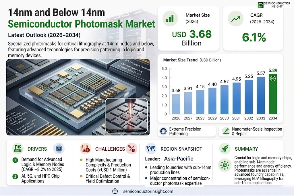
Global 14nm and Below 14nm Semiconductor Photomask Market size was valued at USD 3.42 billion in 2025. The market is projected to grow from USD 3.68 billion in 2026 to USD 5.89 billion by 2034, exhibiting a CAGR of 6.1% during the forecast period.
Semiconductor photomasks are critical components in the fabrication of integrated circuits (ICs), serving as templates for transferring intricate circuit patterns onto silicon wafers. The 14nm and below segment represents advanced node technologies, enabling higher transistor density and improved performance in modern chips. These photomasks include binary masks, phase-shift masks (PSM), and extreme ultraviolet (EUV) masks, catering to applications such as logic devices, memory chips, and foundry services.
The market growth is driven by increasing demand for high-performance computing (HPC), artificial intelligence (AI), and 5G technologies, which require advanced semiconductor nodes. Additionally, rising investments in semiconductor manufacturing capacity expansion by key players like TSMC, Samsung, and Intel are accelerating adoption. However, challenges such as high production costs and stringent defect control requirements may hinder scalability. Leading manufacturers such as Photronics, Toppan, DNP, and SMIC-Mask Service dominate the market with specialized mask solutions tailored for cutting-edge process nodes.
MARKET DRIVERS
Increasing Demand for Advanced Semiconductor Nodes
14nm and Below 14nm Semiconductor Photomask Market is experiencing significant growth due to the rising demand for advanced logic and memory chips. As semiconductor manufacturers push for higher performance and energy efficiency, the adoption of sub-14nm nodes has accelerated. The market is projected to grow at a CAGR of 8.2% until 2025, driven by applications in AI, 5G, and high-performance computing.
Expansion of Foundry Capabilities
Leading foundries are investing heavily in sub-14nm production lines, increasing the need for high-quality photomasks. The complexity of these nodes requires defect-free masks with extreme precision, which is pushing advancements in mask inspection and repair technologies.
The growing adoption of EUV lithography for sub-10nm nodes is further accelerating photomask requirements, as these advanced processes demand tighter specifications and superior mask materials.
MARKET CHALLENGES
High Manufacturing Complexity and Costs
Photomasks for 14nm and below nodes require sophisticated fabrication processes, driving up production costs. The average cost of a sub-14nm photomask can exceed USD 1 million, creating barriers for small and medium-sized semiconductor manufacturers.
Other Challenges
Critical Defect Control
As node sizes shrink, even nanometer-scale defects can cause device failures, requiring stringent inspection and repair processes. Yield optimization remains a key challenge for mass production.
MARKET RESTRAINTS
Limited Number of Advanced Photomask Suppliers
14nm and Below 14nm Semiconductor Photomask Market is dominated by a handful of specialized manufacturers with the technical expertise to meet strict quality requirements. This concentration limits competition and can lead to supply chain bottlenecks for semiconductor companies.
MARKET OPPORTUNITIES
Growth in Edge Computing and IoT Devices
The proliferation of edge computing and IoT applications is creating new demand for energy-efficient, high-performance chips using 14nm and below nodes. Semiconductor photomask manufacturers are well-positioned to benefit from this expanding market segment.
14nm and Below 14nm Semiconductor Photomask Market Trends
Increasing Demand for Advanced Semiconductor Nodes
14nm and Below 14nm Semiconductor Photomask Market is experiencing growth due to rising demand for advanced semiconductor nodes. Leading manufacturers are investing heavily in 7nm and below process technologies to meet the requirements of high-performance computing, 5G networks, and AI applications. This technological progression creates continuous demand for precision photomasks with tighter tolerance specifications.
Other Trends
Supply Chain Optimization
Photomask suppliers are optimizing production processes to maintain yield rates while handling increasingly complex designs. The transition to extreme ultraviolet (EUV) lithography compatible masks for 7nm and below nodes requires specialized manufacturing expertise, creating supply chain challenges that leading players are addressing through strategic partnerships.
Regional Market Developments
Geographically, Asia-Pacific remains the dominant region for 14nm and below photomask production and consumption, particularly in Taiwan, South Korea, and China. The U.S. market maintains strong R&D capabilities, while European manufacturers focus on specialized applications. Trade policies and export controls continue to influence regional supply dynamics in this strategic semiconductor component market.
Competitive Landscape Shifts
The market remains concentrated among established players like Photronics, Toppan, and DNP, who collectively hold significant market share. These companies are expanding production capacity for advanced nodes while smaller players focus on niche applications or regional markets.
Technology Innovation Drive
Continuous innovation in mask-writing technologies and inspection systems is critical for maintaining quality at smaller nodes. The industry is seeing increased adoption of multi-beam mask writers and AI-based defect detection systems to enhance production efficiency for 14nm and below photomasks.
COMPETITIVE LANDSCAPE
Key Industry Players
Leading Suppliers Driving Advanced Node Photomask Innovation
Global 14nm and Below 14nm Semiconductor Photomask Market is dominated by specialized manufacturers with Photronics, Toppan, and DNP collectively holding significant market share. These industry leaders have invested heavily in EUV lithography capabilities to cater to cutting-edge 7nm and 5nm process nodes. Taiwan Semiconductor Manufacturing Company (TSMC) and Samsung Electronics represent major captive mask shop operators vertically integrated with their foundry operations.
Niche players like SMIC-Mask Technology and United Microelectronics Corporation (UMC) focus on regional Chinese markets while maintaining technological partnerships with global IDMs. Emerging Asian suppliers including Nippon Filcon and Hoya Corporation are gaining traction through specialty mask solutions for advanced packaging applications. The market sees increasing R&D collaboration between mask makers and semiconductor equipment vendors to address yield challenges at sub-10nm nodes.
List of Key 14nm and Below Semiconductor Photomask Companies Profiled
- Photronics
- Toppan Photomasks
- Dai Nippon Printing (DNP)
- SMIC-Mask Technology
- Taiwan Semiconductor Manufacturing Company (TSMC)
- Samsung Electronics
- United Microelectronics Corporation (UMC)
- GlobalFoundries
- LG Innotek
- Nippon Filcon
- Hoya Corporation
- Compugraphics Photomask Solutions
- Photronics
- Plasma-Therm
- Intel Corporation
Segment Analysis:
| Segment Category | Sub-Segments | Key Insights |
| By Type |
|
14nm Nodes remains the mainstream technology due to:
|
| By Application |
|
Logic Devices dominate due to:
|
| By End User |
|
Consumer Electronics leads with critical factors:
|
| By Mask Complexity |
|
Multi-Patterning Masks are most prevalent because:
|
| By Geography |
|
Asia-Pacific dominates due to:
|
Regional Analysis: Asia-Pacific 14nm and Below 14nm Semiconductor Photomask Market
Taiwan/South Korea Semiconductor Cluster
Home to 60% of global EUV mask production capacity, the region leads in pellicle development and actinic inspection systems for advanced node photomasks. Mask blank suppliers have established local buffer stocks for critical geometries.
Taiwanese/Korean foundries pioneered AI-based mask defect classification systems, reducing inspection time by 40% while improving detection accuracy for sub-20nm features. Machine learning models continuously update based on production data.
Unique just-in-sequence photomask logistics synchronize mask production with wafer starts. Mask shops receive real-time process updates from foundries to optimize critical dimension uniformity across reticles.
Local research consortia are developing ultra-low thermal expansion substrates and advanced absorber stacks to address stochastic effects in sub-5nm mask patterning, with several materials in pilot production.
North America
The North American 14nm and below photomask market benefits from strong IDM-fabless ecosystem collaboration. Intel’s Oregon and Arizona fabs drive demand for leading-edge masks with specialized OPC requirements. Photomask innovation focuses on computational lithography enhancements, with EDA companies and mask shops co-developing inverse lithography solutions. The region excels in hyperscale computing photomasks requiring tight intra-die CD control. Strategic partnerships between national labs and mask makers explore quantum dot-based mask technologies for post-EUV nodes.
Europe
European semiconductor photomask activity concentrates on specialty applications like automotive and industrial ICs at the 14nm-22nm nodes. Imec’s pilot line serves as collaborative platform for advanced mask R&D, particularly in DUV multi-patterning solutions. The region shows strength in mask-related metrology equipment and resist chemistry development. ASML’s EUV technology base provides proximity advantages in mask pattern fidelity optimization, though wafer-level production remains limited compared to Asia.
China
China’s aggressive semiconductor self-sufficiency push is rapidly expanding 14nm photomask capabilities, though advanced node production still relies on international partners. Domestic mask shops are mastering 193i multiple patterning while building EUV infrastructure. The Yangtze River Delta cluster shows particular strength in display driver and power management IC masks. Government mandates requiring local mask sourcing for certain critical chip applications are reshaping regional supply dynamics.
Rest of World
Emerging photomask activities in Southeast Asia focus on legacy node support and mask requalification services. Israel’s strong position in computational lithography software influences advanced mask design methodologies globally. Limited domestic production exists in Japan for specialty memory and image sensor masks, supported by unique blank substrate technologies. These regions primarily serve as technology feeders to major semiconductor hubs rather than leading-edge volume producers.
Report Scope
This market research report provides a comprehensive analysis of the 14nm and Below 14nm Semiconductor Photomask Market, covering the forecast period 2025–2034. It offers detailed insights into market dynamics, technological advancements, competitive landscape, and key trends shaping the industry.
Key focus areas of the report include:
- Market Overview: The report begins with an overview outlining its current market scenario, key growth indicators, and industry transformation drivers. It discusses macroeconomic factors, demand–supply balance, regulatory landscape, and the strategic role of semiconductors in powering advancements across industries such as automotive, telecommunications, consumer electronics, and industrial automation.
- Market Size & Forecast: Historical data and future projections for revenue, unit shipments, and market value across major regions and segments.
- Segmentation Analysis: Detailed breakdown by product type, technology, application, and end-user industry to identify high-growth segments and investment opportunities.
- Regional Insights: Insights into market performance across North America, Europe, Asia-Pacific, Latin America, and the Middle East & Africa, including country-level analysis where relevant.
- Competitive Landscape: Profiles of leading market participants, including their product offerings, R&D focus, manufacturing capacity, pricing strategies, and recent developments such as mergers, acquisitions, and partnerships.
- Technology Trends & Innovation: Assessment of emerging technologies, integration of AI/IoT, semiconductor design trends, fabrication techniques, and evolving industry standards.
- Market Drivers & Restraints: Evaluation of factors driving market growth along with challenges, supply chain constraints, regulatory issues, and market-entry barriers.
- Stakeholder Insights: Insights for component suppliers, OEMs, system integrators, investors, and policymakers regarding the evolving ecosystem and strategic opportunities.
Primary and secondary research methods are employed, including interviews with industry experts, data from verified sources, and real-time market intelligence to ensure the accuracy and reliability of the insights presented.
FREQUENTLY ASKED QUESTIONS:
What is the current market size of 14nm and Below 14nm Semiconductor Photomask Market?
-> 14nm and Below 14nm Semiconductor Photomask Market size was valued at USD 3.42 billion in 2025. The market is projected to grow from USD 3.68 billion in 2026 to USD 5.89 billion by 2034, exhibiting a CAGR of 6.1% during the forecast period.
Which key companies operate in 14nm and Below 14nm Semiconductor Photomask Market?
-> Key players include Photronics, Toppan, DNP, SMIC-Mask Service, among others.
What are the key growth drivers?
-> Key growth drivers include advanced semiconductor fabrication demand, technological advancements in nodes below 14nm, and increasing applications in consumer electronics and automotive sectors.
Which region dominates the market?
-> Asia-Pacific is the fastest-growing region, with China expected to reach USD million by 2034, while the U.S. market is estimated at USD million in 2025.
What are the emerging trends?
-> Emerging trends include shifts towards 7nm nodes, increasing R&D investments in photomask technologies, and expansion of fabrication capabilities.

Get Sample Report PDF for Exclusive Insights
Report Sample Includes
- Table of Contents
- List of Tables & Figures
- Charts, Research Methodology, and more...
 Download Sample Report PDF