MARKET INSIGHTS
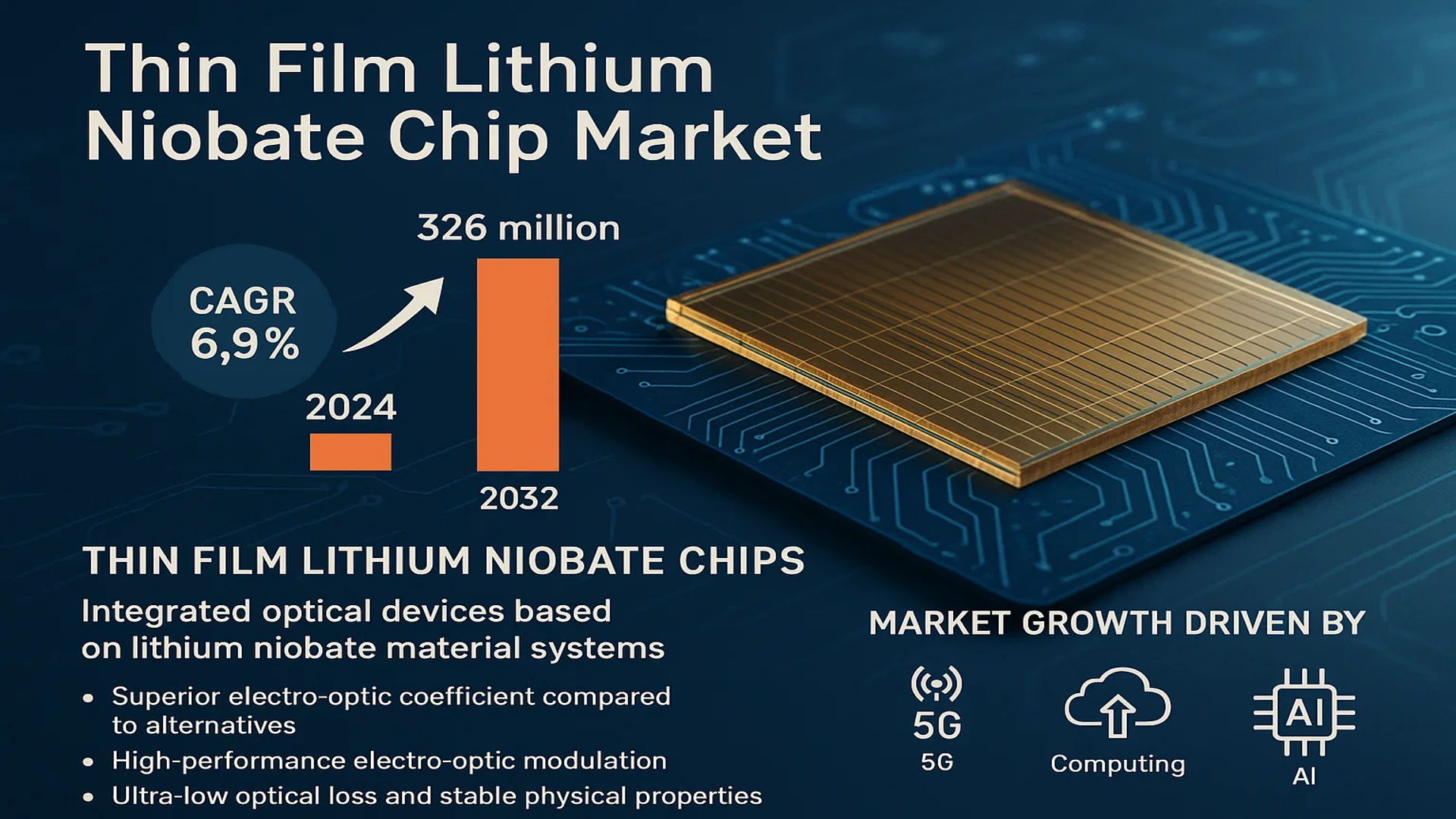
The global Thin Film Lithium Niobate Chip Market was valued at 205 million in 2024 and is projected to reach US$ 326 million by 2032, at a CAGR of 6.9% during the forecast period.
Thin film lithium niobate chips are integrated optical devices based on lithium niobate material systems, known for their superior electro-optic coefficient compared to alternatives like indium phosphide. These chips enable high-performance electro-optic modulation, making them essential components in optical fiber networks and high-speed optoelectronic systems. Their ultra-low optical loss and stable physical properties ensure reliable performance across diverse environments.
The market growth is driven by rising demand for high-speed data transmission in 5G, cloud computing, and AI applications. Technological advancements in micro-nano processing, including electron beam lithography and heterogeneous integration, have enhanced chip performance and integration density. Key players like Fujitsu, Sumitomo, and TSMC are expanding production capabilities to meet growing demand, particularly in optical communication and data center applications.
MARKET DYNAMICS
MARKET DRIVERS
Expansion of 5G and High-Speed Optical Networks Accelerating Adoption
The global rollout of 5G networks necessitates advanced photonic components capable of handling ultra-high bandwidths with low latency. Thin film lithium niobate chips, with electro-optic response speeds exceeding 100 GHz and insertion losses below 3 dB/cm, are becoming indispensable for 5G fronthaul and backbone networks. The ability to process signal modulations above 400Gbps positions these chips as critical enablers for next-generation telecommunications infrastructure. With ongoing 5G deployments across North America, Europe, and Asia-Pacific regions, the addressable market for high-performance optical modulators continues to expand significantly.
Data Center Hyperscaling Demanding Energy-Efficient Photonics
Hyperscale data centers are increasingly adopting thin film lithium niobate solutions for intra-data-center interconnects, where their combination of high bandwidth density and low power consumption addresses critical scaling challenges. Modern chip designs demonstrate power efficiencies below 100 fJ/bit, representing a 60% improvement over conventional silicon photonics solutions. With cloud service providers accelerating construction of new facilities to support AI workloads and edge computing, annual investments in data center optical infrastructure are expected to grow substantially, creating sustained demand for advanced modulator technologies.
➤ Recent industry benchmarks show thin film lithium niobate modulators achieving transmission distances exceeding 80 km without signal regeneration – a critical advantage for distributed computing architectures.
Breakthroughs in Wafer-Scale Fabrication Enhancing Commercial Viability
Advances in ion-slicing and wafer bonding techniques now enable production-scale manufacturing of lithium niobate thin films with sub-200 nm thickness uniformity across 200 mm wafers. This manufacturing scalability directly translates to improved cost structures, with leading foundries achieving 70% yield improvements through optimized dry etch processes. The availability of foundry services through partnerships with major semiconductor manufacturers has significantly lowered barriers to adoption across the supply chain.
MARKET RESTRAINTS
Complex Packaging Requirements Impacting Time-to-Market
The high-performance characteristics of thin film lithium niobate devices create stringent packaging challenges that constrain market growth. Maintaining sub-1 dB fiber coupling losses at the chip interfaces demands precision alignment systems with sub-micron tolerances, often requiring specialized active alignment equipment. These packaging complexities extend development cycles by 30-40% compared to conventional photonic components while adding 25-35% to final assembly costs. The industry continues to seek breakthrough solutions in flip-chip bonding and passive alignment techniques to address these limitations.
Competition from Alternative Material Platforms Creating Price Pressure
Emerging silicon photonics and indium phosphide solutions continue to improve performance while benefiting from established semiconductor manufacturing ecosystems. Though lithium niobate maintains advantages in linearity and bandwidth, competing platforms now achieve comparable metrics in specific applications. This intensifying competition creates pricing pressures, particularly in cost-sensitive datacom segments where performance differentiation proves less critical. Market analysis suggests 15-20% average price erosion is occurring in conventional modulator segments as alternative technologies gain traction.
MARKET CHALLENGES
Thermal Management Limitations in High-Density Integration
The electro-optic performance of lithium niobate exhibits measurable temperature dependence, creating thermal management challenges in high-density photonic integrated circuits. Maintaining operational stability requires active temperature control systems that complicate system architectures. In coherent transceiver applications, thermal crosstalk between adjacent channels can degrade signal integrity, limiting achievable port densities. While novel waveguide designs and thermal isolation structures show promise, these engineering challenges continue to constrain the most demanding integration scenarios.
Other Challenges
Supply Chain Constraints for Specialty Materials
Consistent access to high-quality lithium niobate wafers with optimal crystalline properties remains a persistent challenge. The limited number of qualified substrate suppliers creates potential bottlenecks, particularly during periods of rapid demand growth. Recent geopolitical factors have further complicated raw material supply chains, introducing unpredictability in lead times and pricing stability.
Design Tool Gaps for Complex Photonic ICs
The industry lacks comprehensive electronic-photonic co-design platforms that fully account for lithium niobate’s unique material properties. This tooling gap extends development cycles for sophisticated photonic integrated circuits, as designers must rely on custom simulation approaches and iterative prototyping to achieve target performance metrics.
MARKET OPPORTUNITIES
Emerging Quantum Technologies Creating New Application Horizons
Quantum computing and communications systems are creating new demand vectors for high-performance photonic components. Thin film lithium niobate’s exceptional electro-optic properties make it uniquely suited for quantum light sources, frequency converters, and entanglement distribution systems. Early prototypes demonstrate orders-of-magnitude improvements in quantum state manipulation fidelity compared to conventional approaches. With global quantum technology investments projected for substantial growth, this represents a strategic expansion opportunity.
Heterogeneous Integration Opening System-Level Innovation
Advanced packaging techniques enabling 3D integration of lithium niobate photonics with silicon electronics unlock transformative system architectures. Recent developments in hybrid bonding allow direct integration of photonic and electronic components with sub-micron precision, enabling complete transceiver solutions with unprecedented performance metrics. This integration pathway supports the co-development of application-specific photonic-electronic systems optimized for emerging computing paradigms.
Automotive LiDAR Creating Volume Application Potential
The automotive industry’s transition toward autonomous driving systems creates substantial opportunities for compact, high-performance optical beam steering solutions. Lithium niobate’s fast switching capabilities and optical transparency in near-infrared wavelengths position it as an attractive material for solid-state LiDAR systems. Initial ecosystem partnerships between photonic chip developers and automotive Tier 1 suppliers signal growing interest in leveraging these advantages for next-generation sensing applications.
THIN FILM LITHIUM NIOBATE CHIP MARKET TRENDS
5G and Cloud Computing Expansion to Fuel Market Growth
The global thin film lithium niobate chip market is witnessing accelerated growth due to rising demand from 5G networks and cloud computing infrastructure. With data traffic expected to grow at a compound annual rate of over 25% through 2030, telecom operators are investing heavily in high-speed optical communication systems where these chips play a crucial role. Their ultra-low optical loss and high electro-optic coefficient make them indispensable for next-generation optical modulators capable of handling 800Gbps and beyond. Recent advancements in heterogeneous integration have further enhanced their application in photonic integrated circuits (PICs), particularly for datacenter interconnects where power efficiency is paramount.
Other Trends
Advanced Fabrication Technologies
Breakthroughs in nano-patterning techniques like electron beam lithography with dry etching have enabled mass production of thin film lithium niobate chips with sub-micron precision. The market is seeing increased adoption of wafer-level processing methods that reduce manufacturing costs while improving yield rates. This technological evolution has allowed manufacturers to transition from laboratory-scale production to commercial volumes, with several foundries now offering 200mm wafer processing capabilities.
Emerging Applications in Quantum Computing
Beyond traditional telecommunications, thin film lithium niobate chips are finding novel applications in quantum photonics. Their exceptional non-linear optical properties make them ideal platforms for photon pair generation and quantum state modulation. Research institutions and quantum computing startups are increasingly collaborating with photonic component manufacturers to develop integrated quantum light sources based on this technology. This emerging application segment could account for nearly 15% of the market by 2032, particularly as quantum networks move from experimental to commercial deployment phases.
COMPETITIVE LANDSCAPE
Key Industry Players
Innovation and Partnerships Drive Market Competition in Thin Film Lithium Niobate Technology
The global thin film lithium niobate (TFLN) chip market features a diverse mix of established semiconductor firms and specialized photonics innovators. Fujitsu and Sumitomo maintain strong positions due to their vertical integration capabilities and extensive optical communication product lines. These Japanese giants leverage decades of experience in lithium niobate crystal growth and precision manufacturing.
TSMC (Taiwan Semiconductor Manufacturing Company) has emerged as a critical foundry partner for TFLN chip production, utilizing its advanced 300mm wafer processing capabilities. Their entry into the photonics space through specialized packaging technologies has enabled cost reduction and yield improvements for smaller design firms.
Meanwhile, pure-play photonics companies like HyperLight (USA) and Liobate Technologies Limited (UK) are driving innovation through patented waveguide designs. Their focused R&D on heterogeneous integration with silicon photonics has created new application potential in quantum computing and LiDAR systems.
Several Chinese manufacturers including Advanced Fiber Resources (Zhuhai), Ltd. and Shanghai Anpaixinyan Technology Co., Ltd. are rapidly expanding their production capacity. Government initiatives supporting domestic semiconductor independence have accelerated their technology adoption, though quality inconsistencies remain a challenge in the mid-tier segment.
List of Key Thin Film Lithium Niobate Chip Manufacturers
- Fujitsu (Japan)
- Sumitomo (Japan)
- Advanced Fiber Resources (Zhuhai), Ltd. (China)
- Shanghai Anpaixinyan Technology Co., Ltd. (China)
- LUXTELLIGENCE (France)
- TSMC (Taiwan)
- HyperLight (U.S.)
- Liobate Technologies Limited (UK)
- Ningbo Yuanxin Optoelectronic Technology Co., Ltd. (China)
Segment Analysis:
By Type
High-Speed (>400Gbps) Segment Leads Due to Rising Demand in Optical Communication Networks
The market is segmented based on data transmission speed into:
- High-Speed (>400Gbps)
- Standard (<400Gbps)
By Application
Optical Communication Segment Dominates Owing to Growing 5G and Data Traffic Requirements
The market is segmented based on application into:
- Optical Communication
- Data Center
- Consumer Electronics
- Automotive Electronics
- Others
By Technology
Electron Beam Lithography + Dry Etching is Preferred for High Precision Manufacturing
The market is segmented by fabrication technology into:
- Electron Beam Lithography (EBL) + Dry Etching
- Ultraviolet + Dry Etching
- DUV + Dry Etching
- Other Nano-fabrication Methods
By Integration Method
Heterogeneous Integration Gaining Traction for Hybrid Optical Systems
The market is segmented by integration approach into:
- Heterogeneous Integration
- Monolithic Integration
- Hybrid Integration
Regional Analysis: Thin Film Lithium Niobate Chip Market
Asia-Pacific
The Asia-Pacific region dominates the Thin Film Lithium Niobate Chip market, accounting for over 45% of global demand, driven primarily by China’s rapid 5G deployment and expansive data center construction. China’s national strategy for photonic chip innovation, backed by $1.2 billion in government funding through the 14th Five-Year Plan, has accelerated domestic production capabilities. Japan and South Korea follow closely, with their established semiconductor ecosystems and increasing demand from hyperscale data centers. While cost-competitiveness remains crucial in price-sensitive markets like India, the region benefits from vertically integrated supply chains and strong government-academia-industry collaborations in photonics R&D. However, export controls on advanced lithography equipment present challenges for complete supply chain independence.
North America
North America maintains strong technological leadership in Thin Film Lithium Niobate Chip development, with the U.S. contributing nearly 30% of global R&D investments. The region’s market growth is propelled by defense applications, quantum computing initiatives, and hyperscale data centers demanding ultra-high-speed optical interconnects. Strategic partnerships between companies like HyperLight and academic institutions (e.g., Harvard, MIT) have yielded breakthroughs in heterogenous integration techniques. The CHIPS Act allocation of $52 billion for semiconductor technologies indirectly benefits photonic chip development, though specific funding for lithium niobate remains limited. Regulatory requirements for secure optical communications in government networks create specialized demand segments with stringent performance specifications.
Europe
Europe demonstrates steady growth in the Thin Film Lithium Niobate Chip market, driven by precision instrumentation applications in the automotive and industrial sectors. The EU’s Photonics21 initiative has allocated €700 million to advance integrated photonics, with German and Dutch companies leading in wafer-scale manufacturing techniques. Strict data privacy regulations accelerate adoption in secure communication systems, while the region’s focus on sustainability pushes development of energy-efficient modulator designs. Collaborative projects between research institutions (e.g., IMEC, Fraunhofer) and corporations leverage Europe’s strength in precision engineering, though commercialization lags behind Asia-Pacific and North America due to fragmented production scale.
Middle East & Africa
The MEA region shows emerging potential for Thin Film Lithium Niobate Chips, primarily driven by smart city initiatives in UAE and Saudi Arabia which require advanced optical networking infrastructure. While local manufacturing remains limited, governments are establishing technology transfer partnerships with Asian and European firms to build capabilities. Israel’s strong photonics research ecosystem presents opportunities for specialized applications in defense and medical imaging. Market growth faces challenges including limited local expertise in nanofabrication and dependence on imports for advanced equipment, though sovereign wealth fund investments in digital infrastructure are gradually improving market accessibility.
South America
South America represents a developing market with Brazil and Argentina showing early demand from telecommunications upgrades and academic research institutions. The lack of local fabrication facilities creates complete import dependency, raising costs and limiting market penetration. Brazilian government initiatives like the National Photonics Institute aim to build technical capabilities, while Chile’s astronomy sector drives niche demand for precision optical components. Economic volatility and currency fluctuations hinder large-scale investments in photonic technologies despite growing recognition of their strategic importance for digital transformation.
Report Scope
This market research report provides a comprehensive analysis of the Global Thin Film Lithium Niobate Chip market, covering the forecast period 2025–2032. It offers detailed insights into market dynamics, technological advancements, competitive landscape, and key trends shaping the industry.
Key focus areas of the report include:
- Market Size & Forecast: Historical data and future projections for revenue, unit shipments, and market value across major regions and segments. The Global Thin Film Lithium Niobate Chip market was valued at USD 205 million in 2024 and is projected to reach USD 326 million by 2032, growing at a CAGR of 6.9%.
- Segmentation Analysis: Detailed breakdown by product type (≤400Gbps, >400Gbps), application (Optical Communication, Data Center, Consumer Electronics, Automotive Electronics, Others), and end-user industry to identify high-growth segments.
- Regional Outlook: Insights into market performance across North America, Europe, Asia-Pacific, Latin America, and the Middle East & Africa, with country-level analysis for key markets.
- Competitive Landscape: Profiles of leading market participants including Fujitsu, Sumitomo, Advanced Fiber Resources, TSMC, and HyperLight, covering product portfolios, R&D investments, and strategic developments.
- Technology Trends & Innovation: Assessment of emerging fabrication techniques like electron beam lithography, heterogeneous integration, and ultra-low loss waveguide processing.
- Market Drivers & Restraints: Evaluation of growth drivers including 5G deployment, cloud computing expansion, and AI adoption, along with challenges in manufacturing scalability.
- Stakeholder Analysis: Strategic insights for component suppliers, OEMs, investors, and policymakers regarding the photonic integrated circuits ecosystem.
Primary and secondary research methodologies were employed, including interviews with industry experts and analysis of verified market data, to ensure the accuracy and reliability of findings.
FREQUENTLY ASKED QUESTIONS:
What is the current market size of Global Thin Film Lithium Niobate Chip Market?
-> Thin Film Lithium Niobate Chip Market was valued at 205 million in 2024 and is projected to reach US$ 326 million by 2032, at a CAGR of 6.9% during the forecast period.
Which key companies operate in Global Thin Film Lithium Niobate Chip Market?
-> Key players include Fujitsu, Sumitomo, TSMC, HyperLight, Advanced Fiber Resources (Zhuhai), Ltd., and Shanghai Anpaixinyan Technology Co., Ltd.
What are the key growth drivers?
-> Key growth drivers include 5G infrastructure development, increasing data center demand, and adoption in high-speed optical communication systems.
Which region dominates the market?
-> Asia-Pacific leads the market due to strong semiconductor manufacturing capabilities, while North America shows significant R&D investments.
What are the emerging trends?
-> Emerging trends include wafer-level lithography advancements, heterogeneous integration techniques, and ultra-low loss waveguide development.

Get Sample Report PDF for Exclusive Insights
Report Sample Includes
- Table of Contents
- List of Tables & Figures
- Charts, Research Methodology, and more...