Sputtering Target for Semiconductor Market, Emerging Trends, Technological Advancements, and Business Strategies 2025-2032

Sputtering Target for Semiconductor Market size is projected to grow from USD 1.78 billion in 2024 to USD 3.07 billion by 2032, CAGR of 7.4% during the forecast period

PDF Icon Download Sample Report PDF
  • Quick Dispatch

    All Orders

  • Secure Payment

    100% Secure Payment

Price range: $1,500.00 through $4,250.00

Clear

MARKET INSIGHTS

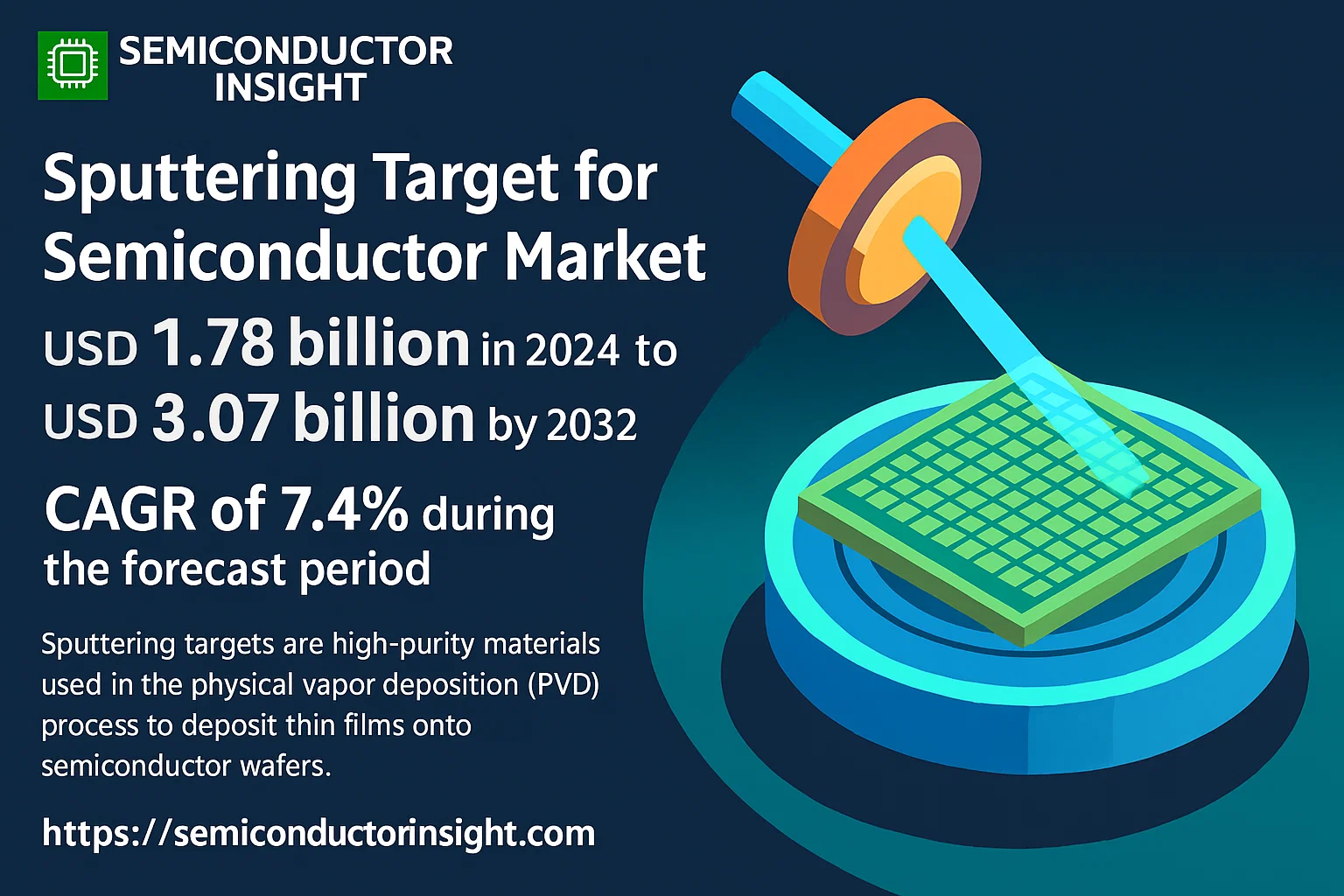
Global Sputtering Target for Semiconductor Market size is projected to grow from USD 1.78 billion in 2024 to USD 3.07 billion by 2032, CAGR of 7.4% during the forecast period.

Sputtering targets are high-purity materials used in the physical vapor deposition (PVD) process to deposit thin films onto semiconductor wafers. These films are critical for fabricating integrated circuits (ICs) and other semiconductor devices. The process involves bombarding a target material with energetic ions, causing atoms to be ejected and deposited as a thin, uniform layer. This technology is essential for creating the intricate and miniaturized structures in modern electronics.

Market growth is primarily driven by the increasing demand for advanced electronics, including smartphones, tablets, and Internet of Things (IoT) devices, which require more powerful and efficient semiconductors. The ongoing miniaturization of semiconductor nodes, such as the transition to 3nm and 2nm processes, necessitates the use of high-performance sputtering targets to deposit precise and defect-free thin films. Additionally, the rise of artificial intelligence (AI), 5G technology, and electric vehicles (EVs) is creating new demand for advanced semiconductors, further propelling the market.

However, the market also faces challenges, including potential supply chain disruptions for critical raw materials like tungsten, cobalt, and copper. Geopolitical tensions and trade restrictions can impact the availability and cost of these materials. Furthermore, the high cost and technical complexity of manufacturing advanced sputtering targets pose barriers to entry for new market participants.

Geographically, the Asia-Pacific region, particularly China, Taiwan, South Korea, and Japan, is expected to remain the largest market due to its dominant position in global semiconductor manufacturing. North America and Europe are also significant markets, supported by government initiatives to bolster domestic semiconductor production capabilities.

Sputtering Target for Semiconductor Market

MARKET DRIVERS

Proliferation of Advanced Semiconductor Devices

The relentless demand for more powerful and efficient semiconductors for applications like artificial intelligence, 5G, and high-performance computing is a primary driver. Sputtering targets are essential for depositing thin, uniform metallic and dielectric films in the fabrication of advanced logic and memory chips. The transition to smaller technology nodes, such as 5nm and 3nm, requires ultra-high purity targets to ensure device performance and yield, directly fueling market growth.

Expansion of the Internet of Things (IoT) Ecosystem

The exponential growth of connected devices is driving the need for a vast quantity of semiconductors, many of which utilize sputtering for thin-film deposition. These semiconductors power sensors, microcontrollers, and communication chips embedded in everything from consumer wearables to industrial equipment. This broad-based demand creates a steady, high-volume requirement for various types of sputtering targets.

Increasing investment in new semiconductor fabrication plants (fabs) globally, particularly for leading-edge logic and memory, is creating a long-term, sustainable demand pipeline for high-performance sputtering targets.

Furthermore, the continual adoption of new interconnect materials, such as cobalt for copper barriers and ruthenium for advanced nodes, is driving the development and consumption of new target materials, presenting significant opportunities for material innovation.

MARKET CHALLENGES

High Cost and Supply Chain Volatility of Raw Materials

The production of high-purity sputtering targets relies on critical raw materials like tantalum, cobalt, and rare earth elements. The prices and availability of these materials are subject to significant geopolitical and supply chain fluctuations. This volatility poses a major challenge for target manufacturers in terms of cost management and securing a stable supply to meet consistent demand from semiconductor fabricators.

Other Challenges

Technical Complexity of Advanced Targets
As chip geometries shrink, the technical specifications for sputtering targets become increasingly stringent. Achieving the required levels of purity (often 99.999% or higher), grain size control, and metallurgical properties demands sophisticated manufacturing processes and significant R&D investment. This high barrier to entry limits the number of qualified suppliers.

Intense Price Pressure from Semiconductor Manufacturers
Semiconductor manufacturers operate in a highly competitive environment and exert substantial pressure on their suppliers, including sputtering target producers, to reduce costs. This constant pressure on pricing can compress profit margins for target manufacturers, challenging their ability to fund necessary research and development for next-generation products.

MARKET RESTRAINTS

Cyclical Nature of the Semiconductor Industry

The sputtering target market is intrinsically linked to the capital expenditure cycles of the semiconductor industry. During periods of downturn or overcapacity, semiconductor manufacturers delay or cancel new equipment purchases and reduce production volumes. This directly translates into reduced demand for sputtering targets, creating periods of significant revenue volatility and uncertainty for target suppliers.

Long and Rigorous Qualification Processes

Introducing a new sputtering target material or a new supplier into a semiconductor fabrication process is an extremely lengthy and costly process. It requires extensive testing and qualification to ensure it meets the strict performance, yield, and reliability standards of the fab. This long lead time acts as a restraint, slowing down the adoption of new materials and making it difficult for new entrants to penetrate the market.

MARKET OPPORTUNITIES

Emergence of New Semiconductor Applications

Beyond traditional computing, new growth frontiers like automotive semiconductors (for electrification and autonomy) and advanced packaging technologies (such as 2.5D/3D integration) present substantial opportunities. These applications require specialized thin-film materials and processes, driving demand for innovative sputtering targets tailored to these specific performance and reliability requirements.

Development of Recyclable and Large-Sized Targets

There is a growing focus on improving the cost-effectiveness and sustainability of the sputtering process. This creates opportunities for manufacturers who can develop larger-sized targets that increase throughput and reduce downtime in fabs, as well as establish efficient recycling programs for used targets. Reclaiming and reprocessing precious metals from spent targets offers both economic and environmental benefits.

Geographical Expansion of Semiconductor Manufacturing

Government initiatives globally, such as the CHIPS Act in the United States and similar programs in Europe and Asia, are incentivizing the construction of new semiconductor manufacturing capacity. This geographical diversification of the supply chain creates new localized demand for sputtering targets, offering growth opportunities for suppliers who can establish a strong presence in these emerging manufacturing hubs.

Sputtering Target for Semiconductor Market Trends
Strong Market Growth Fueled by Semiconductor Demand

The global Sputtering Target for Semiconductor market, valued at $1,781 million in 2024, is projected to reach $3,071 million by 2032, growing at a compound annual growth rate (CAGR) of 7.4%. This robust growth is primarily driven by the relentless advancement in semiconductor technology and increasing demand across multiple high-growth sectors. As semiconductor manufacturing progresses toward smaller process nodes like 3nm, the requirements for high-purity materials become more stringent, directly fueling the demand for specialized sputtering targets. These high-purity materials are essential in the physical vapor deposition (PVD) process to create the precise, uniform thin films that form the functional layers of integrated circuits and memory chips.

Other Trends

Diversified Application Drivers

Beyond the core wafer manufacturing process, sputtering targets are critically important in wafer assembly and testing. In these final production stages, sputtering is used to deposit thin films that enhance the connectivity, protection, and overall functionality of integrated circuits. The demand for these applications is being propelled by the automotive industry’s rapid adoption of electric vehicles (EVs), autonomous driving systems, and advanced driver-assistance systems (ADAS), all of which rely heavily on sophisticated semiconductors. Similarly, the global expansion of 5G networks and the infrastructure required for artificial intelligence (AI) applications are creating substantial demand for advanced semiconductors, further driving the need for high-performance sputtering targets.

Regional Dynamics and Supply Chain Challenges

The Asia-Pacific region dominates market demand, a reflection of its central role in global semiconductor manufacturing, with key contributions from China, Taiwan, South Korea, and Japan. North America and Europe are also poised for significant growth, supported by government initiatives aimed at bolstering domestic semiconductor production capabilities. However, the market faces notable challenges, including supply chain vulnerabilities for critical raw materials like tungsten, molybdenum, and copper. Geopolitical issues and logistical disruptions can lead to cost volatility and production delays. Furthermore, the continuous push for technological miniaturization demands ongoing innovation in sputtering target purity and manufacturing precision, presenting both a challenge and an area for potential advancement.

COMPETITIVE LANDSCAPE

Key Industry Players

A highly specialized market driven by material purity and technological innovation

The global sputtering target for semiconductor market is characterized by the presence of several major multinational corporations and specialized material suppliers, creating a concentrated yet competitive landscape. JX Advanced Metals, Materion, and Konfoong Materials International are recognized as leading players, leveraging extensive R&D capabilities and long-standing relationships with top-tier semiconductor foundries. These companies dominate due to their ability to consistently supply ultra-high purity materials, including metals like tungsten, tantalum, and copper, which are critical for advanced nodes such as 3nm and below. The market structure is evolving as technological complexity increases, pushing for greater vertical integration and strategic partnerships throughout the semiconductor supply chain to ensure material availability and quality control.

Beyond the market leaders, a number of other significant companies hold important niches. Players like Plansee SE and TANAKA are renowned for their expertise in refractory metals and precious metal targets, respectively. Companies such as ULVAC and Honeywell provide essential process expertise alongside their materials. Grinm Advanced Materials Co., Ltd. and Longhua Technology Group highlight the strong presence of Chinese manufacturers in the supply chain. Firms like Furuya Metal and Angstrom Sciences cater to specialized application needs, while established chemical giants like Sumitomo Chemical and Linde (through its electronics gases and materials division) bring significant scale and diverse material portfolios to the market.

List of Key Sputtering Target for Semiconductor Companies Profiled

Segment Analysis:

Segment Category Sub-Segments Key Insights
By Type
  • Metal Sputtering Target Material
  • Alloy Sputtering Target Material
  • Non-metal Sputtering Target Material
Metal Sputtering Target Material holds a dominant position, driven by the extensive use of high-purity metals such as aluminum, copper, and tantalum in depositing critical conductive and barrier layers for semiconductor interconnects. The relentless miniaturization of semiconductor nodes requires metals with exceptional electrical properties and deposition uniformity. While alloys offer tailored properties for specific applications and non-metals like silicon dioxide are essential for dielectric layers, the foundational requirement for superior conductivity and reliability in advanced logic and memory chips solidifies the leadership role of pure metal targets in the market.
By Application
  • Wafer Manufacturing
  • Wafer Assembly and Testing
  • Other Advanced Packaging
Wafer Manufacturing is the primary application segment, as it constitutes the core front-end process where sputtering targets are indispensable for creating the intricate multi-layer thin films that form the transistors and circuits on the silicon wafer. This stage demands the highest levels of material purity and process precision, especially for cutting-edge nodes. The Wafer Assembly and Testing segment is also critical, utilizing targets to deposit films that enhance connectivity and protection in packaging, but the sheer volume and complexity of layers deposited during the initial wafer fabrication process underscore the leading role of the wafer manufacturing application.
By End User
  • Integrated Device Manufacturers (IDMs)
  • Foundries
  • Memory Manufacturers
Foundries represent the most significant end-user segment, acting as the manufacturing hubs for a vast array of fabless semiconductor companies. The intense competition and technological race among leading foundries to produce chips at 5nm, 3nm, and beyond creates sustained, high-volume demand for advanced sputtering targets. While Integrated Device Manufacturers (IDMs) have substantial in-house production needs and Memory Manufacturers are major consumers for DRAM and NAND flash production, the concentrated and scalable nature of the pure-play foundry business model makes it the dominant force driving consumption and technological requirements in the sputtering target market.
By Material Purity Level
  • High Purity (4N to 5N)
  • Ultra High Purity (6N and above)
  • Research Grade Purity
Ultra High Purity (6N and above) targets are increasingly the leading requirement for advanced semiconductor manufacturing. As device geometries shrink to atomic scales, even minute impurities can cause catastrophic failures in yield and performance. This segment is critical for leading-edge logic and memory applications where material consistency and defect-free deposition are non-negotiable. While High Purity grades suffice for some mature nodes and less critical layers, the industry’s trajectory toward more complex architectures is creating a powerful and growing pull for the superior quality and reliability offered by ultra high purity materials.
By Target Form
  • Planar Targets
  • Rotary Targets
  • Bonded Targets
Planar Targets remain the most widely used form factor due to their simplicity, reliability, and suitability for a vast range of semiconductor deposition processes. Their flat geometry allows for uniform erosion and consistent film properties across wafers, which is paramount for high-volume manufacturing. Rotary targets offer improved material utilization for specific applications, and bonded targets are essential for managing thermal stress with high-cost materials, but the foundational role of planar targets in mainstream production tools and processes cements their leading position in the market landscape.

Regional Analysis: Sputtering Target for Semiconductor Market

Asia-Pacific

The Asia-Pacific region is the undisputed global leader in the sputtering target market for semiconductors, driven by its concentration of semiconductor manufacturing and assembly hubs. Countries like Taiwan, South Korea, Japan, and China are the primary engines of growth, hosting the world’s largest foundries and integrated device manufacturers. These nations exhibit exceptionally strong demand for advanced sputtering targets, especially for high-purity metals like copper, aluminum, and titanium, which are essential for manufacturing cutting-edge logic and memory chips. The region’s dominance is underpinned by extensive government support, substantial investments in R&D for next-generation nodes, and a deeply entrenched, sophisticated electronics supply chain. The presence of major target manufacturers within the region further optimizes the supply and development cycle, creating a self-reinforcing ecosystem of innovation and production. This tight integration between material suppliers and semiconductor fabricators gives Asia-Pacific a significant competitive advantage, enabling faster adoption of new materials required for advanced packaging and sub-7nm processes. The region’s focus on maintaining its technological leadership ensures sustained, high-volume demand for sputtering targets.

Manufacturing and Supply Chain Concentration
The region’s unparalleled strength lies in its dense cluster of major semiconductor fabrication plants (fabs). This concentration creates a massive, localized demand for sputtering targets, fostering a highly efficient and responsive supply chain. Proximity to end-users allows for close collaboration on material specifications and rapid problem-solving, which is crucial for high-volume manufacturing. This integrated ecosystem minimizes logistical delays and enhances supply security for critical materials.
Demand for Advanced Node Materials
Asia-Pacific is at the forefront of producing semiconductors at the most advanced technology nodes (e.g., 5nm, 3nm, and below). This leadership drives the demand for highly specialized and ultra-high-purity sputtering targets, including cobalt, ruthenium, and advanced alloys used in transistor gates and interconnects. The relentless push for miniaturization and performance in this region creates a continuous cycle of innovation and requirement for next-generation target materials.
Government and Corporate Investment
Substantial national initiatives and corporate investments are a hallmark of the region. Countries like China, South Korea, and Japan have launched long-term strategic plans and provided significant funding to achieve semiconductor self-sufficiency and technological supremacy. This results in the construction of new fabs and R&D centers, which directly translates into sustained and growing demand for sputtering targets from both established suppliers and emerging local players.
Focus on Advanced Packaging
Beyond front-end fabrication, the region is a global hub for advanced packaging technologies like 2.5D and 3D IC packaging. These packaging techniques require specialized sputtering processes for creating thin films on silicon interposers and through-silicon vias (TSVs). The expertise and scale in packaging within Asia-Pacific generate significant demand for targets used in these specific applications, adding another layer of market strength.

North America
North America remains a critical and technologically advanced region in the sputtering target market, anchored by strong R&D capabilities and the presence of leading semiconductor equipment manufacturers and fabless design companies. The region’s market is characterized by a high demand for specialized, high-value targets used in R&D for next-generation semiconductor architectures and in the production of high-performance chips for computing, AI, and aerospace/defense applications. While its manufacturing capacity is smaller than Asia-Pacific’s, it focuses on low-volume, high-mix production of highly complex chips. Collaborative ecosystems between national laboratories, universities, and companies drive innovation in new target materials. Recent policy initiatives aimed at reshoring semiconductor manufacturing are expected to stimulate future growth in domestic demand for sputtering targets, though the region will continue to rely on its technological leadership and innovation-driven demand.

Europe
Europe holds a significant position in the sputtering target market, distinguished by its strong focus on research, specialization, and high-quality manufacturing. The region is a leader in developing and utilizing targets for specialized semiconductor applications, particularly in the automotive, industrial, and power electronics sectors. European research institutions and companies are at the forefront of developing new materials for MEMS sensors, power semiconductors (like SiC and GaN), and specialized analog chips. The market demand is driven by a need for high-reliability and long-lifecycle components for automotive and industrial systems. Collaborative projects within the EU, such as the Important Project of Common European Interest (IPCEI) on microelectronics, are fostering investment and innovation in the semiconductor supply chain, including advanced materials like sputtering targets, ensuring Europe maintains its niche as a supplier of highly specialized, value-added components.

South America
The sputtering target market in South America is relatively nascent and small-scale compared to other regions, with limited local semiconductor manufacturing infrastructure. Market activity is primarily focused on supporting the consumer electronics assembly industry and some industrial applications. Demand for sputtering targets is largely met through imports, as the region lacks major domestic target manufacturers or advanced semiconductor fabs. However, there is growing interest in developing local technological capabilities, particularly in countries like Brazil. Potential for future growth exists if regional economic stability improves and investments in technology sectors increase, but currently, the market dynamics are defined by its role as a consumer within the global supply chain rather than a significant producer or innovator in the field.

Middle East & Africa
The Middle East & Africa region represents an emerging and potential growth area for the sputtering target market, though it currently accounts for a very small share of global demand. The market is primarily driven by the Middle East, where nations with sovereign wealth funds are making strategic investments in technology diversification beyond oil and gas. This includes plans for building semiconductor-related infrastructure and fostering tech hubs. Any local demand for sputtering targets is currently for maintenance and small-scale operations rather than large-volume production. Africa’s market is minimal, with sporadic activity related to consumer electronics repair and minor industrial applications. The long-term outlook points to gradual growth as these regions continue their economic diversification efforts, but they remain minor players in the current global landscape.

Report Scope

This market research report provides a comprehensive analysis of the Sputtering Target for Semiconductor Market , covering the forecast period 2024–2032. It offers detailed insights into market dynamics, technological advancements, competitive landscape, and key trends shaping the industry.

Key focus areas of the report include:

  • Market Overview: The report begins with an overview outlining its current market scenario, key growth indicators, and industry transformation drivers. It discusses macroeconomic factors, demand–supply balance, regulatory landscape, and the strategic role of semiconductors in powering advancements across industries such as automotive, telecommunications, consumer electronics, and industrial automation.
  • Market Size & Forecast: Historical data and future projections for revenue, unit shipments, and market value across major regions and segments.
  • Segmentation Analysis: Detailed breakdown by product type, technology, application, and end-user industry to identify high-growth segments and investment opportunities.
  • Regional Insights: Insights into market performance across North America, Europe, Asia-Pacific, Latin America, and the Middle East & Africa, including country-level analysis where relevant.
  • Competitive Landscape: Profiles of leading market participants, including their product offerings, R&D focus, manufacturing capacity, pricing strategies, and recent developments such as mergers, acquisitions, and partnerships.
  • Technology Trends & Innovation: Assessment of emerging technologies, integration of AI/IoT, semiconductor design trends, fabrication techniques, and evolving industry standards.
  • Market Drivers & Restraints: Evaluation of factors driving market growth along with challenges, supply chain constraints, regulatory issues, and market-entry barriers.
  • Stakeholder Insights: Insights for component suppliers, OEMs, system integrators, investors, and policymakers regarding the evolving ecosystem and strategic opportunities.

Primary and secondary research methods are employed, including interviews with industry experts, data from verified sources, and real-time market intelligence to ensure the accuracy and reliability of the insights presented.

FREQUENTLY ASKED QUESTIONS:

What is the current market size of Sputtering Target for Semiconductor Market?

-> Global Sputtering Target for Semiconductor Market was valued at USD 1781 million in 2024 and is projected to reach USD 3071 million by 2032, exhibiting a CAGR of 7.4% during the forecast period.

Which key companies operate in Sputtering Target for Semiconductor Market?

-> Key players include JX Advanced Metals, Materion, Konfoong Materials International, Plansee SE, Honeywell, Grinm Advanced Materials Co., Ltd., ULVAC, and TANAKA, among others.

What are the key growth drivers?

-> Key growth drivers include advancements in semiconductor technology, demand for high-performance chips in consumer electronics and automotive sectors, and the expansion of 5G and AI infrastructure.

Which region dominates the market?

-> Asia-Pacific is the dominant market, driven by semiconductor manufacturing hubs in China, Taiwan, South Korea, and Japan.

What are the emerging trends?

-> Emerging trends include the push towards smaller semiconductor nodes (e.g., 3nm), development of high-purity materials, and innovations to meet stringent thin-film requirements.

Sputtering Target for Semiconductor Market, Emerging Trends, Technological Advancements, and Business Strategies 2025-2032

Get Sample Report PDF for Exclusive Insights

Report Sample Includes

  • Table of Contents
  • List of Tables & Figures
  • Charts, Research Methodology, and more...
PDF Icon Download Sample Report PDF

Download Sample Report

Table of Content

1 Introduction to Research & Analysis Reports
1.1 Sputtering Target for Semiconductor Market Definition
1.2 Market Segments
1.2.1 Segment by Type
1.2.2 Segment by Application
1.3 Global Sputtering Target for Semiconductor Market Overview
1.4 Features & Benefits of This Report
1.5 Methodology & Sources of Information
1.5.1 Research Methodology
1.5.2 Research Process
1.5.3 Base Year
1.5.4 Report Assumptions & Caveats
2 Global Sputtering Target for Semiconductor Overall Market Size
2.1 Global Sputtering Target for Semiconductor Market Size: 2024 VS 2031
2.2 Global Sputtering Target for Semiconductor Market Size, Prospects & Forecasts: 2020-2031
2.3 Key Market Trends, Opportunity, Drivers and Restraints
2.3.1 Market Opportunities & Trends
2.3.2 Market Drivers
2.3.3 Market Restraints
3 Company Landscape
3.1 Top Sputtering Target for Semiconductor Players in Global Market
3.2 Top Global Sputtering Target for Semiconductor Companies Ranked by Revenue
3.3 Global Sputtering Target for Semiconductor Revenue by Companies
3.4 Top 3 and Top 5 Sputtering Target for Semiconductor Companies in Global Market, by Revenue in 2024
3.5 Global Companies Sputtering Target for Semiconductor Product Type
3.6 Tier 1, Tier 2, and Tier 3 Sputtering Target for Semiconductor Players in Global Market
3.6.1 List of Global Tier 1 Sputtering Target for Semiconductor Companies
3.6.2 List of Global Tier 2 and Tier 3 Sputtering Target for Semiconductor Companies
4 Sights by Product
4.1 Overview
4.1.1 Segmentation by Type – Global Sputtering Target for Semiconductor Market Size Markets, 2024 & 2031
4.1.2 Metal Sputtering Target Material
4.1.3 Alloy Sputtering Target Material
4.1.4 Non-metal Sputtering Target Material
4.2 Segmentation by Type – Global Sputtering Target for Semiconductor Revenue & Forecasts
4.2.1 Segmentation by Type – Global Sputtering Target for Semiconductor Revenue, 2020-2025
4.2.2 Segmentation by Type – Global Sputtering Target for Semiconductor Revenue, 2026-2031
4.2.3 Segmentation by Type – Global Sputtering Target for Semiconductor Revenue Market Share, 2020-2031
5 Sights by Application
5.1 Overview
5.1.1 Segmentation by Application – Global Sputtering Target for Semiconductor Market Size, 2024 & 2031
5.1.2 Wafer Manufacturing
5.1.3 Wafer Assembly and Testing
5.2 Segmentation by Application – Global Sputtering Target for Semiconductor Revenue & Forecasts
5.2.1 Segmentation by Application – Global Sputtering Target for Semiconductor Revenue, 2020-2025
5.2.2 Segmentation by Application – Global Sputtering Target for Semiconductor Revenue, 2026-2031
5.2.3 Segmentation by Application – Global Sputtering Target for Semiconductor Revenue Market Share, 2020-2031
6 Sights by Region
6.1 By Region – Global Sputtering Target for Semiconductor Market Size, 2024 & 2031
6.2 By Region – Global Sputtering Target for Semiconductor Revenue & Forecasts
6.2.1 By Region – Global Sputtering Target for Semiconductor Revenue, 2020-2025
6.2.2 By Region – Global Sputtering Target for Semiconductor Revenue, 2026-2031
6.2.3 By Region – Global Sputtering Target for Semiconductor Revenue Market Share, 2020-2031
6.3 North America
6.3.1 By Country – North America Sputtering Target for Semiconductor Revenue, 2020-2031
6.3.2 United States Sputtering Target for Semiconductor Market Size, 2020-2031
6.3.3 Canada Sputtering Target for Semiconductor Market Size, 2020-2031
6.3.4 Mexico Sputtering Target for Semiconductor Market Size, 2020-2031
6.4 Europe
6.4.1 By Country – Europe Sputtering Target for Semiconductor Revenue, 2020-2031
6.4.2 Germany Sputtering Target for Semiconductor Market Size, 2020-2031
6.4.3 France Sputtering Target for Semiconductor Market Size, 2020-2031
6.4.4 U.K. Sputtering Target for Semiconductor Market Size, 2020-2031
6.4.5 Italy Sputtering Target for Semiconductor Market Size, 2020-2031
6.4.6 Russia Sputtering Target for Semiconductor Market Size, 2020-2031
6.4.7 Nordic Countries Sputtering Target for Semiconductor Market Size, 2020-2031
6.4.8 Benelux Sputtering Target for Semiconductor Market Size, 2020-2031
6.5 Asia
6.5.1 By Region – Asia Sputtering Target for Semiconductor Revenue, 2020-2031
6.5.2 China Sputtering Target for Semiconductor Market Size, 2020-2031
6.5.3 Japan Sputtering Target for Semiconductor Market Size, 2020-2031
6.5.4 South Korea Sputtering Target for Semiconductor Market Size, 2020-2031
6.5.5 Southeast Asia Sputtering Target for Semiconductor Market Size, 2020-2031
6.5.6 India Sputtering Target for Semiconductor Market Size, 2020-2031
6.6 South America
6.6.1 By Country – South America Sputtering Target for Semiconductor Revenue, 2020-2031
6.6.2 Brazil Sputtering Target for Semiconductor Market Size, 2020-2031
6.6.3 Argentina Sputtering Target for Semiconductor Market Size, 2020-2031
6.7 Middle East & Africa
6.7.1 By Country – Middle East & Africa Sputtering Target for Semiconductor Revenue, 2020-2031
6.7.2 Turkey Sputtering Target for Semiconductor Market Size, 2020-2031
6.7.3 Israel Sputtering Target for Semiconductor Market Size, 2020-2031
6.7.4 Saudi Arabia Sputtering Target for Semiconductor Market Size, 2020-2031
6.7.5 UAE Sputtering Target for Semiconductor Market Size, 2020-2031
7 Companies Profiles
7.1 JX Advanced Metals
7.1.1 JX Advanced Metals Corporate Summary
7.1.2 JX Advanced Metals Business Overview
7.1.3 JX Advanced Metals Sputtering Target for Semiconductor Major Product Offerings
7.1.4 JX Advanced Metals Sputtering Target for Semiconductor Revenue in Global Market (2020-2025)
7.1.5 JX Advanced Metals Key News & Latest Developments
7.2 Materion
7.2.1 Materion Corporate Summary
7.2.2 Materion Business Overview
7.2.3 Materion Sputtering Target for Semiconductor Major Product Offerings
7.2.4 Materion Sputtering Target for Semiconductor Revenue in Global Market (2020-2025)
7.2.5 Materion Key News & Latest Developments
7.3 Konfoong Materials International
7.3.1 Konfoong Materials International Corporate Summary
7.3.2 Konfoong Materials International Business Overview
7.3.3 Konfoong Materials International Sputtering Target for Semiconductor Major Product Offerings
7.3.4 Konfoong Materials International Sputtering Target for Semiconductor Revenue in Global Market (2020-2025)
7.3.5 Konfoong Materials International Key News & Latest Developments
7.4 Linde
7.4.1 Linde Corporate Summary
7.4.2 Linde Business Overview
7.4.3 Linde Sputtering Target for Semiconductor Major Product Offerings
7.4.4 Linde Sputtering Target for Semiconductor Revenue in Global Market (2020-2025)
7.4.5 Linde Key News & Latest Developments
7.5 Proterial
7.5.1 Proterial Corporate Summary
7.5.2 Proterial Business Overview
7.5.3 Proterial Sputtering Target for Semiconductor Major Product Offerings
7.5.4 Proterial Sputtering Target for Semiconductor Revenue in Global Market (2020-2025)
7.5.5 Proterial Key News & Latest Developments
7.6 Plansee SE
7.6.1 Plansee SE Corporate Summary
7.6.2 Plansee SE Business Overview
7.6.3 Plansee SE Sputtering Target for Semiconductor Major Product Offerings
7.6.4 Plansee SE Sputtering Target for Semiconductor Revenue in Global Market (2020-2025)
7.6.5 Plansee SE Key News & Latest Developments
7.7 TOSOH
7.7.1 TOSOH Corporate Summary
7.7.2 TOSOH Business Overview
7.7.3 TOSOH Sputtering Target for Semiconductor Major Product Offerings
7.7.4 TOSOH Sputtering Target for Semiconductor Revenue in Global Market (2020-2025)
7.7.5 TOSOH Key News & Latest Developments
7.8 Honeywell
7.8.1 Honeywell Corporate Summary
7.8.2 Honeywell Business Overview
7.8.3 Honeywell Sputtering Target for Semiconductor Major Product Offerings
7.8.4 Honeywell Sputtering Target for Semiconductor Revenue in Global Market (2020-2025)
7.8.5 Honeywell Key News & Latest Developments
7.9 Grinm Advanced Materials Co., Ltd.
7.9.1 Grinm Advanced Materials Co., Ltd. Corporate Summary
7.9.2 Grinm Advanced Materials Co., Ltd. Business Overview
7.9.3 Grinm Advanced Materials Co., Ltd. Sputtering Target for Semiconductor Major Product Offerings
7.9.4 Grinm Advanced Materials Co., Ltd. Sputtering Target for Semiconductor Revenue in Global Market (2020-2025)
7.9.5 Grinm Advanced Materials Co., Ltd. Key News & Latest Developments
7.10 ULVAC
7.10.1 ULVAC Corporate Summary
7.10.2 ULVAC Business Overview
7.10.3 ULVAC Sputtering Target for Semiconductor Major Product Offerings
7.10.4 ULVAC Sputtering Target for Semiconductor Revenue in Global Market (2020-2025)
7.10.5 ULVAC Key News & Latest Developments
7.11 TANAKA
7.11.1 TANAKA Corporate Summary
7.11.2 TANAKA Business Overview
7.11.3 TANAKA Sputtering Target for Semiconductor Major Product Offerings
7.11.4 TANAKA Sputtering Target for Semiconductor Revenue in Global Market (2020-2025)
7.11.5 TANAKA Key News & Latest Developments
7.12 Sumitomo Chemical
7.12.1 Sumitomo Chemical Corporate Summary
7.12.2 Sumitomo Chemical Business Overview
7.12.3 Sumitomo Chemical Sputtering Target for Semiconductor Major Product Offerings
7.12.4 Sumitomo Chemical Sputtering Target for Semiconductor Revenue in Global Market (2020-2025)
7.12.5 Sumitomo Chemical Key News & Latest Developments
7.13 Luvata
7.13.1 Luvata Corporate Summary
7.13.2 Luvata Business Overview
7.13.3 Luvata Sputtering Target for Semiconductor Major Product Offerings
7.13.4 Luvata Sputtering Target for Semiconductor Revenue in Global Market (2020-2025)
7.13.5 Luvata Key News & Latest Developments
7.14 Advantec
7.14.1 Advantec Corporate Summary
7.14.2 Advantec Business Overview
7.14.3 Advantec Sputtering Target for Semiconductor Major Product Offerings
7.14.4 Advantec Sputtering Target for Semiconductor Revenue in Global Market (2020-2025)
7.14.5 Advantec Key News & Latest Developments
7.15 Longhua Technology Group (Luoyang)
7.15.1 Longhua Technology Group (Luoyang) Corporate Summary
7.15.2 Longhua Technology Group (Luoyang) Business Overview
7.15.3 Longhua Technology Group (Luoyang) Sputtering Target for Semiconductor Major Product Offerings
7.15.4 Longhua Technology Group (Luoyang) Sputtering Target for Semiconductor Revenue in Global Market (2020-2025)
7.15.5 Longhua Technology Group (Luoyang) Key News & Latest Developments
7.16 Furuya Metal
7.16.1 Furuya Metal Corporate Summary
7.16.2 Furuya Metal Business Overview
7.16.3 Furuya Metal Sputtering Target for Semiconductor Major Product Offerings
7.16.4 Furuya Metal Sputtering Target for Semiconductor Revenue in Global Market (2020-2025)
7.16.5 Furuya Metal Key News & Latest Developments
7.17 Umicore Thin Film Products
7.17.1 Umicore Thin Film Products Corporate Summary
7.17.2 Umicore Thin Film Products Business Overview
7.17.3 Umicore Thin Film Products Sputtering Target for Semiconductor Major Product Offerings
7.17.4 Umicore Thin Film Products Sputtering Target for Semiconductor Revenue in Global Market (2020-2025)
7.17.5 Umicore Thin Film Products Key News & Latest Developments
7.18 Angstrom Sciences
7.18.1 Angstrom Sciences Corporate Summary
7.18.2 Angstrom Sciences Business Overview
7.18.3 Angstrom Sciences Sputtering Target for Semiconductor Major Product Offerings
7.18.4 Angstrom Sciences Sputtering Target for Semiconductor Revenue in Global Market (2020-2025)
7.18.5 Angstrom Sciences Key News & Latest Developments
8 Conclusion
9 Appendix
9.1 Note
9.2 Examples of Clients
9.3 DisclaimerList of Tables
Table 1. Sputtering Target for Semiconductor Market Opportunities & Trends in Global Market
Table 2. Sputtering Target for Semiconductor Market Drivers in Global Market
Table 3. Sputtering Target for Semiconductor Market Restraints in Global Market
Table 4. Key Players of Sputtering Target for Semiconductor in Global Market
Table 5. Top Sputtering Target for Semiconductor Players in Global Market, Ranking by Revenue (2024)
Table 6. Global Sputtering Target for Semiconductor Revenue by Companies, (US$, Mn), 2020-2025
Table 7. Global Sputtering Target for Semiconductor Revenue Share by Companies, 2020-2025
Table 8. Global Companies Sputtering Target for Semiconductor Product Type
Table 9. List of Global Tier 1 Sputtering Target for Semiconductor Companies, Revenue (US$, Mn) in 2024 and Market Share
Table 10. List of Global Tier 2 and Tier 3 Sputtering Target for Semiconductor Companies, Revenue (US$, Mn) in 2024 and Market Share
Table 11. Segmentation by Type – Global Sputtering Target for Semiconductor Revenue, (US$, Mn), 2024 & 2031
Table 12. Segmentation by Type – Global Sputtering Target for Semiconductor Revenue (US$, Mn), 2020-2025
Table 13. Segmentation by Type – Global Sputtering Target for Semiconductor Revenue (US$, Mn), 2026-2031
Table 14. Segmentation by Application– Global Sputtering Target for Semiconductor Revenue, (US$, Mn), 2024 & 2031
Table 15. Segmentation by Application – Global Sputtering Target for Semiconductor Revenue, (US$, Mn), 2020-2025
Table 16. Segmentation by Application – Global Sputtering Target for Semiconductor Revenue, (US$, Mn), 2026-2031
Table 17. By Region– Global Sputtering Target for Semiconductor Revenue, (US$, Mn), 2024 & 2031
Table 18. By Region – Global Sputtering Target for Semiconductor Revenue, (US$, Mn), 2020-2025
Table 19. By Region – Global Sputtering Target for Semiconductor Revenue, (US$, Mn), 2026-2031
Table 20. By Country – North America Sputtering Target for Semiconductor Revenue, (US$, Mn), 2020-2025
Table 21. By Country – North America Sputtering Target for Semiconductor Revenue, (US$, Mn), 2026-2031
Table 22. By Country – Europe Sputtering Target for Semiconductor Revenue, (US$, Mn), 2020-2025
Table 23. By Country – Europe Sputtering Target for Semiconductor Revenue, (US$, Mn), 2026-2031
Table 24. By Region – Asia Sputtering Target for Semiconductor Revenue, (US$, Mn), 2020-2025
Table 25. By Region – Asia Sputtering Target for Semiconductor Revenue, (US$, Mn), 2026-2031
Table 26. By Country – South America Sputtering Target for Semiconductor Revenue, (US$, Mn), 2020-2025
Table 27. By Country – South America Sputtering Target for Semiconductor Revenue, (US$, Mn), 2026-2031
Table 28. By Country – Middle East & Africa Sputtering Target for Semiconductor Revenue, (US$, Mn), 2020-2025
Table 29. By Country – Middle East & Africa Sputtering Target for Semiconductor Revenue, (US$, Mn), 2026-2031
Table 30. JX Advanced Metals Corporate Summary
Table 31. JX Advanced Metals Sputtering Target for Semiconductor Product Offerings
Table 32. JX Advanced Metals Sputtering Target for Semiconductor Revenue (US$, Mn) & (2020-2025)
Table 33. JX Advanced Metals Key News & Latest Developments
Table 34. Materion Corporate Summary
Table 35. Materion Sputtering Target for Semiconductor Product Offerings
Table 36. Materion Sputtering Target for Semiconductor Revenue (US$, Mn) & (2020-2025)
Table 37. Materion Key News & Latest Developments
Table 38. Konfoong Materials International Corporate Summary
Table 39. Konfoong Materials International Sputtering Target for Semiconductor Product Offerings
Table 40. Konfoong Materials International Sputtering Target for Semiconductor Revenue (US$, Mn) & (2020-2025)
Table 41. Konfoong Materials International Key News & Latest Developments
Table 42. Linde Corporate Summary
Table 43. Linde Sputtering Target for Semiconductor Product Offerings
Table 44. Linde Sputtering Target for Semiconductor Revenue (US$, Mn) & (2020-2025)
Table 45. Linde Key News & Latest Developments
Table 46. Proterial Corporate Summary
Table 47. Proterial Sputtering Target for Semiconductor Product Offerings
Table 48. Proterial Sputtering Target for Semiconductor Revenue (US$, Mn) & (2020-2025)
Table 49. Proterial Key News & Latest Developments
Table 50. Plansee SE Corporate Summary
Table 51. Plansee SE Sputtering Target for Semiconductor Product Offerings
Table 52. Plansee SE Sputtering Target for Semiconductor Revenue (US$, Mn) & (2020-2025)
Table 53. Plansee SE Key News & Latest Developments
Table 54. TOSOH Corporate Summary
Table 55. TOSOH Sputtering Target for Semiconductor Product Offerings
Table 56. TOSOH Sputtering Target for Semiconductor Revenue (US$, Mn) & (2020-2025)
Table 57. TOSOH Key News & Latest Developments
Table 58. Honeywell Corporate Summary
Table 59. Honeywell Sputtering Target for Semiconductor Product Offerings
Table 60. Honeywell Sputtering Target for Semiconductor Revenue (US$, Mn) & (2020-2025)
Table 61. Honeywell Key News & Latest Developments
Table 62. Grinm Advanced Materials Co., Ltd. Corporate Summary
Table 63. Grinm Advanced Materials Co., Ltd. Sputtering Target for Semiconductor Product Offerings
Table 64. Grinm Advanced Materials Co., Ltd. Sputtering Target for Semiconductor Revenue (US$, Mn) & (2020-2025)
Table 65. Grinm Advanced Materials Co., Ltd. Key News & Latest Developments
Table 66. ULVAC Corporate Summary
Table 67. ULVAC Sputtering Target for Semiconductor Product Offerings
Table 68. ULVAC Sputtering Target for Semiconductor Revenue (US$, Mn) & (2020-2025)
Table 69. ULVAC Key News & Latest Developments
Table 70. TANAKA Corporate Summary
Table 71. TANAKA Sputtering Target for Semiconductor Product Offerings
Table 72. TANAKA Sputtering Target for Semiconductor Revenue (US$, Mn) & (2020-2025)
Table 73. TANAKA Key News & Latest Developments
Table 74. Sumitomo Chemical Corporate Summary
Table 75. Sumitomo Chemical Sputtering Target for Semiconductor Product Offerings
Table 76. Sumitomo Chemical Sputtering Target for Semiconductor Revenue (US$, Mn) & (2020-2025)
Table 77. Sumitomo Chemical Key News & Latest Developments
Table 78. Luvata Corporate Summary
Table 79. Luvata Sputtering Target for Semiconductor Product Offerings
Table 80. Luvata Sputtering Target for Semiconductor Revenue (US$, Mn) & (2020-2025)
Table 81. Luvata Key News & Latest Developments
Table 82. Advantec Corporate Summary
Table 83. Advantec Sputtering Target for Semiconductor Product Offerings
Table 84. Advantec Sputtering Target for Semiconductor Revenue (US$, Mn) & (2020-2025)
Table 85. Advantec Key News & Latest Developments
Table 86. Longhua Technology Group (Luoyang) Corporate Summary
Table 87. Longhua Technology Group (Luoyang) Sputtering Target for Semiconductor Product Offerings
Table 88. Longhua Technology Group (Luoyang) Sputtering Target for Semiconductor Revenue (US$, Mn) & (2020-2025)
Table 89. Longhua Technology Group (Luoyang) Key News & Latest Developments
Table 90. Furuya Metal Corporate Summary
Table 91. Furuya Metal Sputtering Target for Semiconductor Product Offerings
Table 92. Furuya Metal Sputtering Target for Semiconductor Revenue (US$, Mn) & (2020-2025)
Table 93. Furuya Metal Key News & Latest Developments
Table 94. Umicore Thin Film Products Corporate Summary
Table 95. Umicore Thin Film Products Sputtering Target for Semiconductor Product Offerings
Table 96. Umicore Thin Film Products Sputtering Target for Semiconductor Revenue (US$, Mn) & (2020-2025)
Table 97. Umicore Thin Film Products Key News & Latest Developments
Table 98. Angstrom Sciences Corporate Summary
Table 99. Angstrom Sciences Sputtering Target for Semiconductor Product Offerings
Table 100. Angstrom Sciences Sputtering Target for Semiconductor Revenue (US$, Mn) & (2020-2025)
Table 101. Angstrom Sciences Key News & Latest Developments

List of Figures
Figure 1. Sputtering Target for Semiconductor Product Picture
Figure 2. Sputtering Target for Semiconductor Segment by Type in 2024
Figure 3. Sputtering Target for Semiconductor Segment by Application in 2024
Figure 4. Global Sputtering Target for Semiconductor Market Overview: 2024
Figure 5. Key Caveats
Figure 6. Global Sputtering Target for Semiconductor Market Size: 2024 VS 2031 (US$, Mn)
Figure 7. Global Sputtering Target for Semiconductor Revenue: 2020-2031 (US$, Mn)
Figure 8. The Top 3 and 5 Players Market Share by Sputtering Target for Semiconductor Revenue in 2024
Figure 9. Segmentation by Type – Global Sputtering Target for Semiconductor Revenue, (US$, Mn), 2024 & 2031
Figure 10. Segmentation by Type – Global Sputtering Target for Semiconductor Revenue Market Share, 2020-2031
Figure 11. Segmentation by Application – Global Sputtering Target for Semiconductor Revenue, (US$, Mn), 2024 & 2031
Figure 12. Segmentation by Application – Global Sputtering Target for Semiconductor Revenue Market Share, 2020-2031
Figure 13. By Region – Global Sputtering Target for Semiconductor Revenue Market Share, 2020-2031
Figure 14. By Country – North America Sputtering Target for Semiconductor Revenue Market Share, 2020-2031
Figure 15. United States Sputtering Target for Semiconductor Revenue, (US$, Mn), 2020-2031
Figure 16. Canada Sputtering Target for Semiconductor Revenue, (US$, Mn), 2020-2031
Figure 17. Mexico Sputtering Target for Semiconductor Revenue, (US$, Mn), 2020-2031
Figure 18. By Country – Europe Sputtering Target for Semiconductor Revenue Market Share, 2020-2031
Figure 19. Germany Sputtering Target for Semiconductor Revenue, (US$, Mn), 2020-2031
Figure 20. France Sputtering Target for Semiconductor Revenue, (US$, Mn), 2020-2031
Figure 21. U.K. Sputtering Target for Semiconductor Revenue, (US$, Mn), 2020-2031
Figure 22. Italy Sputtering Target for Semiconductor Revenue, (US$, Mn), 2020-2031
Figure 23. Russia Sputtering Target for Semiconductor Revenue, (US$, Mn), 2020-2031
Figure 24. Nordic Countries Sputtering Target for Semiconductor Revenue, (US$, Mn), 2020-2031
Figure 25. Benelux Sputtering Target for Semiconductor Revenue, (US$, Mn), 2020-2031
Figure 26. By Region – Asia Sputtering Target for Semiconductor Revenue Market Share, 2020-2031
Figure 27. China Sputtering Target for Semiconductor Revenue, (US$, Mn), 2020-2031
Figure 28. Japan Sputtering Target for Semiconductor Revenue, (US$, Mn), 2020-2031
Figure 29. South Korea Sputtering Target for Semiconductor Revenue, (US$, Mn), 2020-2031
Figure 30. Southeast Asia Sputtering Target for Semiconductor Revenue, (US$, Mn), 2020-2031
Figure 31. India Sputtering Target for Semiconductor Revenue, (US$, Mn), 2020-2031
Figure 32. By Country – South America Sputtering Target for Semiconductor Revenue Market Share, 2020-2031
Figure 33. Brazil Sputtering Target for Semiconductor Revenue, (US$, Mn), 2020-2031
Figure 34. Argentina Sputtering Target for Semiconductor Revenue, (US$, Mn), 2020-2031
Figure 35. By Country – Middle East & Africa Sputtering Target for Semiconductor Revenue Market Share, 2020-2031
Figure 36. Turkey Sputtering Target for Semiconductor Revenue, (US$, Mn), 2020-2031
Figure 37. Israel Sputtering Target for Semiconductor Revenue, (US$, Mn), 2020-2031
Figure 38. Saudi Arabia Sputtering Target for Semiconductor Revenue, (US$, Mn), 2020-2031
Figure 39. UAE Sputtering Target for Semiconductor Revenue, (US$, Mn), 2020-2031
Figure 40. JX Advanced Metals Sputtering Target for Semiconductor Revenue Year Over Year Growth (US$, Mn) & (2020-2025)
Figure 41. Materion Sputtering Target for Semiconductor Revenue Year Over Year Growth (US$, Mn) & (2020-2025)
Figure 42. Konfoong Materials International Sputtering Target for Semiconductor Revenue Year Over Year Growth (US$, Mn) & (2020-2025)
Figure 43. Linde Sputtering Target for Semiconductor Revenue Year Over Year Growth (US$, Mn) & (2020-2025)
Figure 44. Proterial Sputtering Target for Semiconductor Revenue Year Over Year Growth (US$, Mn) & (2020-2025)
Figure 45. Plansee SE Sputtering Target for Semiconductor Revenue Year Over Year Growth (US$, Mn) & (2020-2025)
Figure 46. TOSOH Sputtering Target for Semiconductor Revenue Year Over Year Growth (US$, Mn) & (2020-2025)
Figure 47. Honeywell Sputtering Target for Semiconductor Revenue Year Over Year Growth (US$, Mn) & (2020-2025)
Figure 48. Grinm Advanced Materials Co., Ltd. Sputtering Target for Semiconductor Revenue Year Over Year Growth (US$, Mn) & (2020-2025)
Figure 49. ULVAC Sputtering Target for Semiconductor Revenue Year Over Year Growth (US$, Mn) & (2020-2025)
Figure 50. TANAKA Sputtering Target for Semiconductor Revenue Year Over Year Growth (US$, Mn) & (2020-2025)
Figure 51. Sumitomo Chemical Sputtering Target for Semiconductor Revenue Year Over Year Growth (US$, Mn) & (2020-2025)
Figure 52. Luvata Sputtering Target for Semiconductor Revenue Year Over Year Growth (US$, Mn) & (2020-2025)
Figure 53. Advantec Sputtering Target for Semiconductor Revenue Year Over Year Growth (US$, Mn) & (2020-2025)
Figure 54. Longhua Technology Group (Luoyang) Sputtering Target for Semiconductor Revenue Year Over Year Growth (US$, Mn) & (2020-2025)
Figure 55. Furuya Metal Sputtering Target for Semiconductor Revenue Year Over Year Growth (US$, Mn) & (2020-2025)
Figure 56. Umicore Thin Film Products Sputtering Target for Semiconductor Revenue Year Over Year Growth (US$, Mn) & (2020-2025)
Figure 57. Angstrom Sciences Sputtering Target for Semiconductor Revenue Year Over Year Growth (US$, Mn) & (2020-2025)