
Key Statistics
Key Takeaways
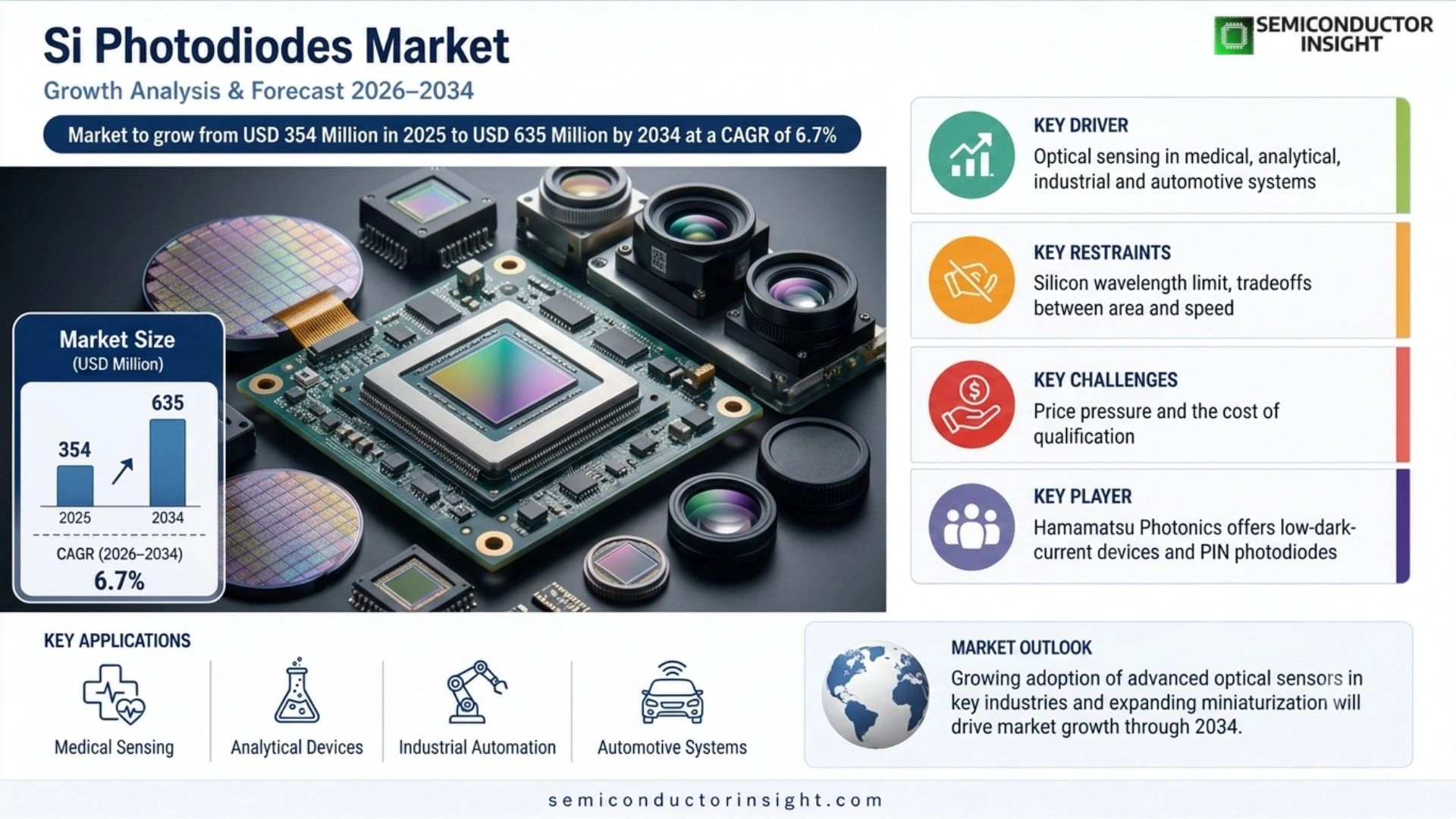
- The rebased market was valued at USD 354 million in 2025 across conventional silicon photodiodes, PIN devices and silicon avalanche photodiodes.
- Revenue is forecast to reach USD 635 million by 2034, representing a 6.7% CAGR during 2026–2034.
- Asia Pacific leads through Japanese photonics expertise, Chinese electronics manufacturing and broad regional demand from instrumentation, consumer, automotive and industrial systems.
- Si PIN photodiodes form the largest commercial category, while avalanche devices, filtered UV detectors and integrated receiver modules provide higher-value growth.
Si Photodiodes Market Overview
Si photodiodes market covers silicon p-n photodiodes, PIN photodiodes and silicon avalanche photodiodes that convert incident ultraviolet, visible or near-infrared light into electrical current. Rebased from the published 2023 and 2030 anchors, the market is valued at USD 354 million in 2025 and forecast to reach USD 635 million by 2034 at a 6.7% CAGR during 2026–2034. Hamamatsu’s product overview distinguishes low-dark-current devices from PIN photodiodes designed for faster response, illustrating how device structure maps to measurement requirements.
Commercial selection depends on spectral responsivity, active area, junction capacitance, dark current, noise, linearity, reverse-voltage behavior, temperature coefficient, rise time, package window and optical geometry. Silicon provides useful response from ultraviolet through visible light and into the near infrared, but sensitivity declines near its long-wavelength limit. LASER COMPONENTS’ Si APD guidance places silicon avalanche devices across approximately 260–1100 nm. The detector must be evaluated with its amplifier, filters, optics and calibration because system noise and stray light can dominate the diode specification.
Segment Analysis: By Type
Type segmentation follows junction architecture and internal gain. Standard p-n devices serve cost-sensitive light measurement, PIN structures reduce capacitance and improve speed, and avalanche photodiodes provide internal multiplication for weak or fast signals. Arrays and position-sensitive variants combine multiple elements for spatial information. Value per unit rises with active-area control, low noise, spectral filtering, qualification and integration into receiver modules.
| Type | Role in the market | Commercial outlook |
|---|---|---|
| Standard Si Photodiodes | Planar p-n devices convert light to current with low complexity and can be operated in photovoltaic or reverse-biased mode. | Broad use in ambient-light, control and general instrumentation applications; pricing is competitive and differentiation centers on dark current, responsivity and package options. |
| Si PIN Photodiodes | A wider intrinsic region reduces junction capacitance and supports faster, more linear detection over UV, visible and near-infrared wavelengths. | Largest commercial category across power meters, encoders, analytical instruments, medical sensing and optical receivers. |
| Si Avalanche Photodiodes (APDs) | Reverse bias near breakdown creates internal gain, improving sensitivity for weak or time-critical optical signals. | Higher-value growth in LiDAR, photon counting, laser measurement and scientific instruments, balanced against bias, temperature and noise complexity. |
| Arrays and Position-Sensitive Devices | Multiple silicon elements provide spatial, quadrant, line or position information and may be supplied with filters or amplification. | Specialized growth in spectrometers, alignment, imaging and industrial measurement where integration reduces system size and calibration effort. |
Segment Analysis: By Application
Applications range from high-volume sensing to traceable scientific measurement. Optical power meters and analytical instruments value linearity and calibration; displays and ambient-light systems emphasize low cost and spectral matching; medical devices require stable signal quality and regulatory evidence; LiDAR and laser systems prioritize speed and low-light sensitivity. The fastest revenue growth is expected where custom filters, arrays or integrated electronics raise content per design.
| Application | Purchase logic | Forecast implications |
|---|---|---|
| Optical Power Meters and Laser Monitoring | Detectors measure source output, beam stability and received optical power in laboratories, manufacturing and communications. | Stable high-value demand tied to calibration, linearity, active-area geometry and wavelength-specific responsivity. |
| Spectrophotometers and Analytical Instruments | Photodiodes and arrays convert dispersed light into quantitative chemical, environmental or process measurements. | Growth follows compact instruments, real-time monitoring and life-science automation; low dark current and long-term stability justify premium devices. |
| Medical and Wearable Sensing | Pulse oximetry, photoplethysmography, diagnostics and imaging use silicon sensitivity across red, visible and near-infrared bands. | Large opportunity with demanding signal-to-noise, package, biocompatibility and regulatory validation requirements. |
| Automotive, Industrial and Consumer Sensors | Ambient-light control, encoders, smoke detection, proximity, safety curtains and selected LiDAR architectures use discrete or array detectors. | High unit volume and qualification-driven design wins; price pressure is offset by automotive reliability, filtered packages and integrated receiver functions. |
| LCD Backlight and Color Adjustment | Photodiodes monitor brightness and spectral balance in displays, illumination and imaging equipment. | Mature but durable application, with miniaturization and surface-mount integration supporting replacement and redesign cycles. |
Regional Analysis
Asia Pacific leads through Japanese photonics suppliers and large electronics, automotive and instrumentation manufacturing bases in China, South Korea and Taiwan. North America remains strong in scientific, medical, aerospace and laser systems, while Europe combines industrial metrology, automotive and photonics expertise. South America and Middle East & Africa are primarily downstream and distribution markets, with selective opportunities in healthcare, environmental monitoring, energy and research.
North America
North America accounts for a substantial high-value share through medical devices, laboratory instrumentation, aerospace, defense, laser systems and industrial sensing. The United States hosts OSI Optoelectronics, Thorlabs, Excelitas operations, Edmund Optics and specialist integrators. NIST optical metrology work supports the traceability environment behind calibrated photodetector systems. Canada adds photonics research and medical technology, while Mexico’s electronics and automotive production creates volume demand for qualified surface-mount detectors.
| Country / market | Commercial role | Evidence-led outlook |
|---|---|---|
| United States | Largest regional buyer and supplier base | Medical, scientific, defense and industrial systems support premium devices. |
| Canada | Research and life-science niche | Photonics institutes and medical innovation create specialized demand. |
| Mexico | Electronics manufacturing market | Automotive and appliance assembly favors qualified, cost-effective detectors. |
Dated market instances
Europe
Europe combines photonics suppliers, automotive engineering, industrial automation, aerospace, medical instruments and scientific laboratories. Germany is a center for detector manufacturing and laser applications, the United Kingdom supports optical instrumentation and distribution, and France, Switzerland and the Netherlands add research and precision systems. Photonics21 coordinates European photonics priorities, helping connect component development with industrial adoption. Compliance, traceability and long product lifecycles favor suppliers that provide detailed application data and stable packaging.
| Country / market | Commercial role | Evidence-led outlook |
|---|---|---|
| Germany | Leading supplier and industrial market | Laser systems, automation and automotive testing sustain advanced photodiodes. |
| United Kingdom | Instrumentation and distribution hub | Research, defense and life sciences support broad catalog and custom demand. |
| France | Aerospace and scientific market | National laboratories and transport industries use qualified optical detectors. |
| Switzerland | Precision-instrument niche | Analytical and metrology systems favor high-linearity components. |
Dated market instances
Asia Pacific
Asia Pacific leads because Japan combines Hamamatsu Photonics, Kyosemi and other detector expertise with demanding instrumentation and automotive customers. China provides large electronics and industrial-sensor manufacturing, while South Korea and Taiwan add displays, semiconductor equipment and consumer devices. India and Southeast Asia expand medical, environmental and industrial demand. Regional scale supports both commodity devices and sophisticated APDs, though high-end customers still require documented dark current, reliability, spectral response and lot consistency.
| Country / market | Commercial role | Evidence-led outlook |
|---|---|---|
| Japan | Technology and supplier leader | Photonics, analytical instruments and automotive systems support premium product development. |
| China | Largest volume manufacturing base | Consumer, industrial and medical electronics create broad detector demand. |
| South Korea | Display and electronics market | High-volume devices and semiconductor manufacturing support compact photodiodes. |
| Taiwan | Electronics and instrument ecosystem | Contract manufacturing and optical modules create diversified demand. |
| India | Emerging medical and industrial market | Diagnostics, automation and environmental monitoring broaden adoption. |
Dated market instances
South America
South American demand is led by Brazil’s healthcare, industrial automation, environmental monitoring and research sectors. Argentina and Chile contribute scientific and resource-industry applications, while distributors provide access to imported detector portfolios. The region has limited large-scale silicon photodiode fabrication, so exchange rates, inventory and technical support influence purchasing. Opportunities are strongest in instruments and modules that simplify optical alignment and calibration for laboratories, water monitoring, mining and medical diagnostics.
| Country / market | Commercial role | Evidence-led outlook |
|---|---|---|
| Brazil | Largest regional opportunity | Medical devices, universities and industrial automation support diverse demand. |
| Argentina | Scientific and medical niche | Research institutes and instrumentation users purchase specialist detectors. |
| Chile | Mining and environmental market | Optical analysis and safety systems create project-based demand. |
| Colombia | Healthcare and process-monitoring market | Imported instruments drive replacement and service demand. |
Dated market instances
Middle East & Africa
Middle East & Africa demand is project-led. Gulf states invest in healthcare, research, smart infrastructure and environmental monitoring, while South Africa supports mining, laboratories and medical equipment. Israel has a strong optoelectronics and defense-technology ecosystem. Much of the region depends on imported components and instruments, so application support and distributor inventory are important. Harsh temperature, dust and sunlight conditions make spectral filtering, package sealing, calibration stability and carefully designed optical paths especially valuable.
| Country / market | Commercial role | Evidence-led outlook |
|---|---|---|
| United Arab Emirates | Research and healthcare hub | Laboratories and smart-infrastructure projects favor integrated sensors. |
| Saudi Arabia | Large project market | Healthcare, energy and environmental programs create instrument demand. |
| Israel | Optoelectronics design center | Defense, medical and imaging companies use specialized photodetectors. |
| South Africa | Mining and laboratory base | Analytical and safety systems support rugged detector demand. |
Dated market instances
Key Si Photodiode Manufacturers and Competitive Landscape
The market includes vertically integrated photonics manufacturers, specialist detector companies, scientific-component suppliers and optical distributors. The source-page company set is retained in full. Competition depends on noise, responsivity, speed, active-area control, spectral customization, packaging, automotive or medical qualification, calibration support and the ability to maintain identical devices over long instrument lifecycles. Custom filters, arrays and integrated amplifiers provide differentiation beyond bare-die price.
| Competitive tier | Companies | Basis of position |
|---|---|---|
| Global detector technology leaders | Hamamatsu Photonics; Excelitas Technologies; OSI Optoelectronics; First Sensor | Broad silicon detector portfolios, process control, application engineering and global qualification support. |
| Specialist manufacturers | Kyosemi; Pioneer Micro Technology; Opto Diode / Illinois Tool Works; Luna Optoelectronics | Custom geometries, radiation and aerospace products, niche process expertise and application-specific packaging. |
| Photonics catalog and integration providers | Thorlabs; LASER COMPONENTS; Edmund Optics; AP Technologies | Wide optical catalogs, rapid availability, technical support, modules and access to research and OEM customers. |
Companies covered in the report
- Hamamatsu Photonics
- Kyosemi
- OSI Optoelectronics
- Pioneer Micro Technology
- Thorlabs Inc.
- LASER COMPONENTS
- Illinois Tool Works Inc. (Opto Diode)
- Edmund Optics
- Excelitas Technologies
- AP Technologies
- First Sensor
- Luna Optoelectronics
Hamamatsu competes through a deep catalog spanning conventional photodiodes, PIN devices, APDs, arrays and amplified modules, supported by extensive application documentation. Excelitas and OSI address medical, industrial, aerospace and scientific requirements, while First Sensor and Opto Diode emphasize qualified specialist designs. Kyosemi, Pioneer Micro Technology and Luna Optoelectronics provide additional custom capability. Product continuity and lot consistency are especially important because redesigning optics, amplifiers and calibration can cost far more than the detector itself.
Thorlabs, LASER COMPONENTS, Edmund Optics and AP Technologies influence purchasing by combining detectors with optical components, modules, evaluation tools and technical distribution. Their advantage is speed of selection and integration, while vertically integrated OEMs may prefer direct custom relationships. Competition is increasingly system-oriented: a lower-capacitance diode may require a smaller active area, and a filtered package may eliminate external optics. Suppliers win when they help customers optimize the complete signal path rather than quoting one isolated parameter.
Detector Selection, Calibration and Optical-System Analysis
Production-capacity analysis is not the most decision-relevant standalone section for Si photodiodes because performance and commercial fit depend on detector physics, optical coupling, amplifier design, calibration and environmental qualification. This replacement examines how spectral response, noise, speed, active area and packaging trade against one another in the complete measurement channel, which is the practical basis for component selection and supplier differentiation.
| Design factor | Qualification requirement | Commercial consequence |
|---|---|---|
| Spectral response | Responsivity and filter transmission at the actual source wavelengths | Determines usable signal and whether silicon is preferable to another detector material. |
| Noise and dark current | Temperature-dependent dark current, shot noise and amplifier noise | Sets minimum detectable power and calibration stability. |
| Speed and capacitance | Junction capacitance, bias, active area and transimpedance bandwidth | Creates a tradeoff between collection area, rise time and receiver complexity. |
| Package and optics | Window material, angle, alignment, sealing and surface-mount process | Affects assembly yield, stray light and long-term field reliability. |
| Calibration and linearity | Traceable responsivity, saturation behavior and drift | Enables quantitative instruments and regulated applications. |
Active area trades against speed and noise
A larger photodiode captures more light and relaxes alignment tolerance, but it generally has higher junction capacitance. Higher capacitance increases amplifier noise gain and can reduce bandwidth. Designers can use reverse bias, smaller areas, focusing optics or integrated transimpedance amplifiers, but each changes cost and risk. Excelitas’ VTH3020 release illustrates a 100 mm² device aimed at applications where collection area is valuable.
Wavelength determines detector architecture
Silicon has strong utility from ultraviolet through visible and into the near infrared, but device thickness, surface treatment and coatings influence the response curve. UV detection may require enhanced surfaces and filters, while 1064 nm YAG sensing operates near silicon’s long-wavelength edge. Hamamatsu’s S17348 description shows how high reverse voltage and device design are used to improve speed at 1060 nm. Beyond silicon’s useful range, InGaAs or other materials become necessary.
APD gain requires controlled bias and temperature
Avalanche photodiodes multiply photocurrent internally, improving sensitivity for weak light and fast timing. Gain also introduces excess noise and varies strongly with reverse voltage and temperature. Receiver design therefore needs stable bias, compensation and protection from overload. APDs should be compared at the system detection threshold and bandwidth rather than by gain alone. Integrated receivers can reduce engineering effort, but they make amplifier bandwidth, recovery and package thermal behavior part of the component qualification.
Calibration must represent the assembled optical path
A diode responsivity certificate does not include losses or spectral changes from windows, filters, lenses, fibers and contamination in the final instrument. Quantitative systems should calibrate the assembled channel at relevant wavelengths and power levels and verify linearity, repeatability and temperature behavior. Traceability is important for power meters, spectrophotometers and medical measurements. Suppliers can create value through calibrated modules, reference detectors, aging data and clear uncertainty budgets that reduce customer validation work.
Si Photodiodes Market Dynamics: Drivers, Restraints and Opportunities
Growth is driven by optical sensing in medical, analytical, industrial and automotive systems, along with miniaturization and application-specific packaging. Restraints include silicon’s wavelength limit, tradeoffs between area and speed, price pressure and the cost of qualification. The directional impact ranges below are scenario estimates relative to the baseline and are not separate market forecasts.
MARKET DRIVERS
Estimated impact of primary growth drivers
| Factor | Directional CAGR impact | Most exposed market | Time horizon |
|---|---|---|---|
| Medical and wearable optical sensing | +1.0 to +1.6 percentage points | Global device OEMs | Medium term |
| Analytical and environmental instruments | +0.8 to +1.3 percentage points | Industrial and laboratory | Medium term |
| Automotive and industrial optical sensing | +0.6 to +1.1 percentage points | Asia, Europe, North America | Medium term |
| Filtered and integrated detector modules | +0.4 to +0.8 percentage points | OEM instrumentation | Immediate to medium |
Optical health sensing is expanding
Pulse oximetry, photoplethysmography, diagnostic analyzers and fluorescence instruments use stable photodetection to convert weak optical signals into physiological measurements. Growth comes from both clinical equipment and wearables, but performance cannot be inferred from a diode alone. Wavelength selection, LED drive, tissue path, motion rejection and algorithms all matter. Photodiode vendors benefit when higher sensitivity, compact packaging or integrated amplification allows OEMs to improve signal quality within power and space constraints.
Compact analytical instruments require reliable detectors
Environmental, chemical, food, semiconductor and life-science instruments increasingly move measurements closer to the process. Silicon photodiodes and arrays can support UV-visible absorption, scattering, fluorescence and source monitoring in compact systems. Demand grows when automation requires more measurement points and when real-time results avoid laboratory delay. Suppliers that provide low-dark-current devices, linear response, filters and long-term availability help instrument makers reduce calibration burden and field-service risk.
Automation and safety add optical channels
Encoders, light curtains, smoke detectors, object sensors, laser monitors and machine-vision subsystems use photodiodes because they are compact, linear and compatible with inexpensive silicon electronics. Factory automation increases the number of optical channels, while functional safety and uptime raise qualification requirements. Surface-mount packaging and integrated receivers reduce assembly cost. Growth is strongest when an optical solution provides a clear reliability or precision advantage over mechanical, capacitive or camera-based alternatives.
Application-specific packaging raises value
A bare detector may require external filters, shielding, amplification and precision alignment. Suppliers can integrate daylight-blocking filters, narrow-band UV filters, arrays, transimpedance amplifiers or rugged windows to solve a larger part of the customer’s problem. Hamamatsu’s S16495 integrates a 310 nm bandpass filter to reject unwanted visible and near-infrared light. Such integration can improve repeatability and justify higher value per design.
MARKET RESTRAINTS
Estimated impact of primary restraints
| Factor | Directional CAGR impact | Most exposed market | Time horizon |
|---|---|---|---|
| Wavelength limits of silicon | -0.8 to -1.2 percentage points | Telecom and mid-IR applications | Structural |
| Area-speed-noise tradeoffs | -0.6 to -1.0 percentage points | High-speed receivers | Medium term |
| Commodity price pressure | -0.5 to -0.9 percentage points | Consumer and basic sensing | Immediate |
| Qualification and redesign cost | -0.4 to -0.8 percentage points | Medical and automotive | Medium term |
Silicon cannot cover every optical band
Silicon responsivity falls near the 1100 nm region and does not serve common long-haul telecom wavelengths around 1310 and 1550 nm. InGaAs and other materials therefore capture applications beyond silicon’s spectral range. UV performance also requires special surface and window engineering. Vendors must define the useful response under real packaging and temperature conditions and avoid overstating broad wavelength labels. The constraint is fundamental, though improved structures can enhance performance near the edges.
Detector parameters involve unavoidable tradeoffs
Large active area improves collection but raises capacitance; reverse bias improves speed but increases dark current and demands control; avalanche gain improves sensitivity but adds excess noise and temperature dependence. Customers may compare one headline specification without seeing the system penalty elsewhere. Suppliers need application notes, SPICE models and evaluation modules to help designers choose a balanced operating point. Poor early selection can force an amplifier, optics or enclosure redesign late in qualification.
High-volume categories face pricing pressure
Standard ambient-light and control photodiodes are available from multiple suppliers and are often a small line item in a larger system. OEMs seek cost reductions and dual sources, limiting margins. Differentiation through filters, qualification, package geometry and stable delivery can protect value, but custom features also reduce scale. Suppliers must manage a broad catalog without accumulating slow-moving inventory while preserving long product lifetimes for industrial and medical customers that resist component changes.
Qualification makes adoption slow
Automotive, medical, aerospace and quantitative instruments require reliability testing, documentation and system validation. A new detector may improve sensitivity but change active area, capacitance, spectral curve or mechanical alignment enough to require substantial retesting. This slows supplier switching and new-product adoption. It also favors vendors with change-control discipline and long availability. Designers should qualify second sources early where feasible, but exact optical and electrical equivalence is often more difficult than matching package pins.
MARKET OPPORTUNITIES
Integrated photodiode receivers
Combining a detector with transimpedance amplification, bias control, temperature compensation and shielding can shorten design time and improve reproducibility. Integrated modules are attractive in medical, analytical and laser-monitoring systems where analog expertise is limited. Vendors can differentiate through low noise, overload recovery and calibration. The design must still expose enough information for system validation and offer stable supply because replacing an integrated receiver can require both electronics and software changes.
Filtered UV and wavelength-selective devices
Water quality, flame sensing, sterilization monitoring and industrial photometry benefit from rejecting ambient or out-of-band light. Thin-film filters placed at the detector can reduce optical assembly and alignment. Custom spectral response creates higher value but requires coating durability, angle characterization and manufacturing consistency. Suppliers with detector and filter expertise can develop application-specific components that occupy less space and deliver more repeatable response than discrete optical stacks.
Silicon APDs and photon-counting arrays
LiDAR, fluorescence, particle analysis and scientific instruments need sensitivity to weak or fast optical events. Silicon APDs and arrays provide internal gain across relevant UV-visible-near-infrared wavelengths. Opportunities include lower noise, better 905 nm and 1064 nm response, compact arrays and integrated quenching or timing electronics. Commercial success depends on temperature control, uniformity, safe bias operation and credible lifetime data as much as on peak photon-detection efficiency.
Automotive and industrial qualification
Qualified surface-mount photodiodes can win long-lived programs in encoders, safety systems, cabin sensing and optical controls. AEC-Q101 evidence, wide temperature operation, controlled change notification and automated assembly compatibility reduce OEM risk. Suppliers can add value through side-view packages, daylight filters and matched emitters. The opportunity is attractive because qualification creates switching costs, but winning designs requires early engineering support and the ability to deliver consistent products for many years.
Photodetection System Ecosystem Analysis
A generic supply-chain section is replaced by a photodetection system ecosystem analysis because commercial value is created through the interaction of detector physics, optical components, analog electronics, calibration and the final instrument. Component availability matters, but buyers make decisions according to signal quality and validation in the assembled channel. The ecosystem view therefore better explains design wins and defensible supplier positions.
Detector suppliers capture more value when they solve adjacent optical and electronic problems. A filtered photodiode can eliminate a separate coating or filter mount; an amplified module can reduce noise and board-design risk; a calibrated assembly can shorten instrument validation. Optical distributors and catalog suppliers create value through availability and component matching, while direct manufacturers support custom geometry and qualification. The commercial boundary is therefore fluid, and comparisons should separate bare-die price from the total engineering, assembly and calibration cost of a working receiver.
Long lifecycle coordination is critical. A window coating change, die shrink or package-tool transfer can alter responsivity, capacitance or alignment even if the part number remains stable. Medical, aerospace and analytical OEMs need change notification, traceability and samples for requalification. Suppliers must also coordinate upstream silicon processes and downstream packaging, filters and test equipment. Buyers can reduce risk with approved alternates, documented optical tolerances and incoming checks, but exact second sourcing is difficult when custom active areas or spectral filters define system performance.
Recent Developments in the Si Photodiodes Market
Developments tracked to September 2026. Entries are dated to their official announcement or publication period.
- April 2026
Source – Hamamatsu announced the S15152 Si PIN photodiode for high-speed optical measurement, free-space optical communication and dimensional analysis in a compact surface-mount-compatible package. - April 2026
Source – Hamamatsu announced a new Si PIN photodiode for high-speed YAG-laser detection, extending silicon performance near the 1064 nm region used in measurement and ranging. - November 2025
Source – Vishay introduced a silicon PIN photodiode with a smaller package and enhanced visible-light sensitivity for biomedical applications. - September 2025
Source – Hamamatsu introduced the S16495 with an integrated 310 nm bandpass filter, targeting selective UV measurement while rejecting visible and near-infrared stray light. - January 2025
Source – Excelitas introduced the VTH3020 chip-on-board large-area silicon photodiode with a 100 mm² active area for advanced optical sensing applications.
REPORT SCOPE & SEGMENTATION
| Attribute | Details |
|---|---|
| Category | Optoelectronics > Photodetectors > Silicon Photodiodes, PIN Photodiodes and APDs |
| Base Year | 2025 |
| Forecast Period | 2026–2034 |
| Market Size | USD 354 million in 2025; USD 635 million by 2034; 6.7% CAGR during 2026–2034 |
| By Type | Standard Si Photodiode; Si PIN Photodiode; Si Avalanche Photodiode; Arrays and Position-Sensitive Devices |
| By Application | Optical Power Meters; LCD Backlight and Color Adjustment; Sunlight Sensors; Spectrophotometers; Medical and Wearable Sensing; Automotive and Industrial Sensors; Other Applications |
| By Spectral Use | Ultraviolet-Enhanced; Visible-Light; Near-Infrared; Filtered Narrow-Band |
| By Package | Bare Die; Through-Hole; Surface-Mount; Optical Module; Integrated Amplified Receiver |
| By Customer | Instrument OEMs; Medical Device OEMs; Automotive and Industrial OEMs; Laboratories; Distributors and Integrators |
| Regions | North America; Europe; Asia Pacific; South America; Middle East & Africa |
| Companies | Hamamatsu Photonics; Kyosemi; OSI Optoelectronics; Pioneer Micro Technology; Thorlabs Inc.; LASER COMPONENTS; Illinois Tool Works Inc. (Opto Diode); Edmund Optics; Excelitas Technologies; AP Technologies; First Sensor; Luna Optoelectronics |
Frequently Asked Questions
What is the current size of the Si photodiodes market?
The global Si photodiodes market was valued at USD 354 million in 2025 after rebasing the source report’s 2023 and 2030 anchors at their implied annual growth rate. The scope includes standard silicon photodiodes, PIN devices, silicon avalanche photodiodes and relevant arrays. It excludes detectors based principally on InGaAs, germanium or other non-silicon absorber materials and excludes complete instruments beyond directly integrated receiver content.
What will the market be worth by 2034?
The market is forecast to reach USD 635 million by 2034, representing a 6.7% CAGR during 2026–2034. Growth is supported by medical optical sensing, compact analytical instruments, industrial automation, automotive detectors, filtered UV products and higher-value APDs. Annual demand can vary with electronics production, customer qualification schedules, instrument capital spending and whether silicon remains technically suitable at the required wavelength, speed and sensitivity.
Which region leads the market?
Asia Pacific is the largest market because Japan combines leading photodiode suppliers and advanced instruments, while China, South Korea and Taiwan provide large electronics, automotive, display and industrial manufacturing bases. North America and Europe retain substantial high-value demand in medical, scientific, defense and precision measurement. Regional shares differ by whether the analysis emphasizes commodity unit volume, specialized detector revenue or integrated receiver modules.
Which product type is most important?
Si PIN photodiodes form the largest commercial segment because the intrinsic region supports low capacitance, fast response and useful linearity across a wide range of optical power meters, encoders, analytical instruments, medical sensors and receivers. Standard devices remain important for low-cost sensing, while silicon APDs and arrays offer faster value growth in LiDAR, photon counting, laser measurement and spatial detection where internal gain or multiple elements justify higher prices.
How should a Si photodiode be selected?
Selection should begin with source wavelength, expected optical power, bandwidth, active-area and alignment needs, temperature and package environment. Engineers then compare responsivity, dark current, junction capacitance, linearity, reverse-bias limits and noise with the intended transimpedance amplifier. Filters, windows and optics must be included. The best component is the one that meets the complete system detection and calibration requirement, not necessarily the diode with the highest single datasheet value.
What are the primary market drivers?
Primary drivers include optical health monitoring, automated analytical instruments, factory sensing, automotive electronics, laser power measurement and application-specific packaging. Miniaturized surface-mount devices lower assembly cost, while integrated filters and amplifiers can improve repeatability. Demand grows as equipment adds more optical channels and as real-time measurements move closer to patients, production lines and environmental processes instead of relying on periodic centralized laboratory analysis.
What are the main restraints?
The main restraints are silicon’s long-wavelength cutoff, parameter tradeoffs between active area, speed and noise, commodity pricing pressure, and slow qualification in medical, automotive, aerospace and analytical systems. APDs add bias and temperature complexity. A detector substitution can alter optics, amplifier stability and calibration, so even technically superior products may take time to adopt. Market growth also depends on reliable packaging, coating and long-lifecycle change control.
Which companies are covered in the report?
The report covers Hamamatsu Photonics, Kyosemi, OSI Optoelectronics, Pioneer Micro Technology, Thorlabs, LASER COMPONENTS, Illinois Tool Works through Opto Diode, Edmund Optics, Excelitas Technologies, AP Technologies, First Sensor and Luna Optoelectronics. Profiles compare device architecture, spectral range, active-area options, noise and speed, filters and modules, qualification support, custom capability, distribution reach and end-market position.
Why was production-capacity analysis replaced?
Production capacity was replaced with detector-selection, calibration and optical-system analysis because customer outcomes depend more directly on responsivity, dark current, capacitance, amplifier noise, filters, alignment and calibration than on aggregate factory output. The replacement explains the engineering tradeoffs that create defensible design wins and lifecycle value. Manufacturing continuity remains relevant within company and ecosystem analysis, but capacity alone does not determine suitability or market adoption.
Where are the strongest opportunities?
The strongest opportunities are integrated low-noise receivers, wavelength-selective and UV-filtered devices, silicon APDs and photon-counting arrays, automotive-qualified surface-mount packages, and calibrated modules for compact medical or environmental instruments. Suppliers can differentiate through custom active areas, long-term stability, change control and application engineering. The greatest value is created when integration removes optical alignment, analog design or calibration work from the customer’s system rather than merely reducing bare-die cost.

Get Sample Report PDF for Exclusive Insights
Report Sample Includes
- Table of Contents
- List of Tables & Figures
- Charts, Research Methodology, and more...
 Download Sample Report PDF


