Key Statistics
Key Takeaways
- Grade I ultra-high-purity polysilicon is the most demanding product tier because leading-edge wafer manufacturers require impurity control at parts-per-billion to parts-per-trillion levels.
- 300mm wafer production is the largest application because advanced logic, DRAM, NAND and high-volume specialty semiconductor fabs use 300mm silicon substrates.
- Asia Pacific is the leading regional market through the concentration of silicon-wafer manufacturing and semiconductor fabs in Japan, South Korea, Taiwan and China.
- Supply is highly concentrated. Tokuyama, WACKER, Hemlock Semiconductor, OCI and other established producers compete through extreme purity, cleaning, packaging and stable long-term qualification rather than commodity pricing.
- Capacity is expanding for semiconductor demand. WACKER increased hyperpure semiconductor-grade cleaning capacity by more than 50%, Tokuyama opened its Vietnam semiconductor-polysilicon plant in August 2026, and OCI is building a broader supply chain around its 4,700-ton Gunsan operation.
Semiconductor Grade Polysilicon Market Overview
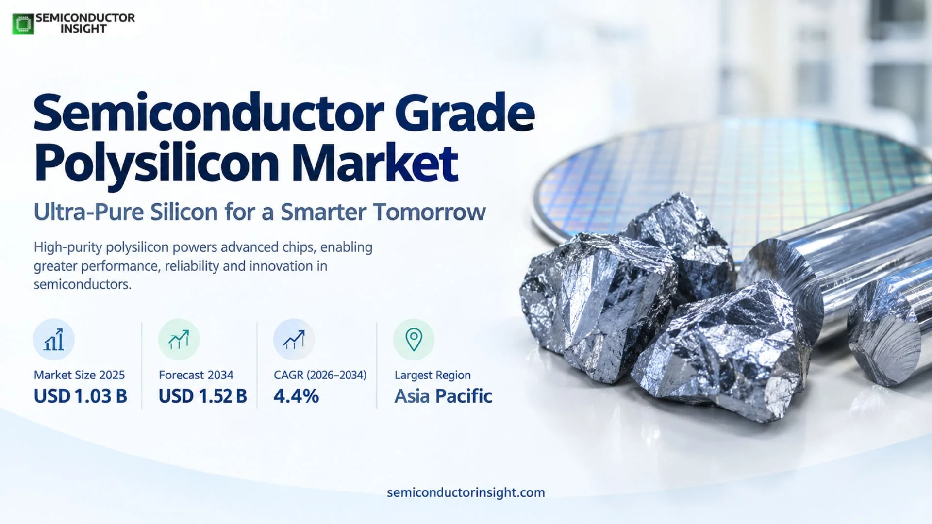
Semiconductor Grade Polysilicon market is valued at USD 1.03 billion in 2025 and is projected to reach USD 1.52 billion by 2034, representing a 4.4% CAGR during 2026–2034. The 2026 estimated market size is USD 1.07 billion. Asia Pacific is the leading regional market because it contains the largest concentration of silicon-wafer manufacturers and semiconductor fabs.
Semiconductor-grade polysilicon is the ultra-pure silicon feedstock used to grow single-crystal ingots for electronic wafers. Purity requirements are dramatically higher than ordinary metallurgical silicon because trace boron, phosphorus, metals and carbon can alter wafer resistivity, minority-carrier behavior and device reliability. Commercial electronic grades commonly reach 9N to 11N purity, with leading suppliers operating beyond those levels for the most demanding applications.
Production generally starts with metallurgical silicon converted into volatile chlorosilanes such as trichlorosilane. Repeated distillation removes impurities before chemical vapor deposition forms high-purity polysilicon rods. The rods are then crushed, etched, cleaned, inspected and packaged in tightly controlled environments so the final material can be used by crystal growers without reintroducing contamination.
Market value is determined not only by installed tonnage but by the fraction of output that can meet semiconductor qualification. Solar-grade material cannot be substituted directly because semiconductor customers require much tighter control of elemental impurities, surface contamination, particle generation and lot consistency. This makes purification, cleaning and quality systems central competitive capabilities.
Segment Analysis: By Type
By type, the market is segmented into Grade I, Grade II and Grade III. Grade I represents the highest-purity category and is most important for advanced semiconductor wafers, while lower grades serve less demanding electronic and specialty applications.
| Grade | Purity / quality role | Market position |
|---|---|---|
| Grade I | Highest-purity material with the tightest control of electrically active and metallic impurities. Producers use advanced distillation, Siemens-process deposition, clean crushing, etching and contamination-controlled packaging. | Premium segment. Leading-edge 300mm logic and memory wafers require the strongest impurity and lot-consistency performance. |
| Grade II | High-purity electronic material suitable for broad semiconductor wafer production where specifications remain stringent but are less extreme than premium leading-edge requirements. | Large mainstream electronic-grade segment supporting 200mm and selected 300mm applications. |
| Grade III | Electronic or specialty-grade material for mature semiconductor, research or less contamination-sensitive applications. | Smaller value segment with broader specification tolerance and stronger price sensitivity. |
Purity, product-form and end-user segmentation
The market can also be segmented by purity, product form and customer class. Nugget, cut-rod and chip forms are selected to match crystal-puller charging systems. Silicon-wafer manufacturers are the principal end users because they convert polysilicon into monocrystalline ingots before slicing and polishing wafers.
| Axis | Segments | Commercial implication |
|---|---|---|
| By Purity / Product Form | 9N–10N · 11N+ · Nugget · S-Nugget · Cut-Rod · Chip / Chunk | Higher purity commands premium pricing and tighter packaging controls; product form affects crystal-puller loading, handling and contamination risk. |
| By End User | Silicon Wafer Manufacturers · IDMs / Captive Crystal Operations · Research / Specialty Users | Wafer manufacturers dominate volume and qualification; captive operations and specialty users create smaller application-specific demand. |
Segment Analysis: By Application
By application, the market is segmented into 300mm Wafers, 200mm Wafers and Other Sizes. 300mm wafer production is the leading application because most advanced logic and memory fabs operate on 300mm substrates.
| Application | Key market insight |
|---|---|
| 300mm Wafers | The largest application. Advanced logic, DRAM, NAND and high-volume specialty fabs require extremely consistent single-crystal ingots, making feedstock purity and lot stability critical. |
| 200mm Wafers | Automotive, analog, power, MEMS and mature-node IC production maintains a large 200mm installed base. These wafers still require electronic-grade feedstock but may use different resistivity and oxygen specifications. |
| 150mm / Specialty Wafers | Compound-device support, research and specialty silicon applications create smaller demand for customized ingot diameter, resistivity or crystal orientation. |
| Advanced Logic & Memory | AI processors, HBM-related DRAM and high-density NAND increase the economic value of defect-free wafers and therefore strengthen demand for ultra-pure feedstock. |
| Automotive & Power | Long-life automotive and industrial devices support stable 200mm and selected 300mm wafer demand, creating durable electronic-grade polysilicon consumption. |
Regional Analysis
Asia Pacific leads the Semiconductor Grade Polysilicon market because Japan, South Korea, Taiwan and China form the core of the semiconductor wafer and device manufacturing supply chain. North America remains strategically important through Hemlock Semiconductor and domestic fab investment, while Europe has a major supplier base through WACKER.
How do semiconductor-grade polysilicon supply and demand differ by region?
Production is concentrated among a small number of highly qualified suppliers, while demand follows silicon-wafer and semiconductor-fab locations. Japan and Germany are major technology centers, South Korea and Taiwan are large semiconductor consumption hubs, and North America is investing in domestic supply resilience.
| Region | Market position | Growth outlook | Core demand | Commercial priority |
|---|---|---|---|---|
| Asia Pacific | Leading | High | 300mm wafers, memory & foundry | Purity, qualification and local supply |
| North America | Strategic supply market | Moderate to high | Domestic fabs & wafer production | Resilience and hyperpure quality |
| Europe | Major supplier region | Moderate to high | Hyperpure polysilicon & specialty wafers | Energy efficiency and premium quality |
| South America | Small | Selective | Research / downstream electronics | Local wafer base |
| Middle East & Africa | Emerging | Selective | Future semiconductor projects | Wafer-manufacturing ecosystem |
Competitive Landscape
Key participants include Tokuyama, WACKER Chemie, Hemlock Semiconductor, Mitsubishi Materials, OSAKA Titanium Technologies, OCI, REC Silicon, GCL-related suppliers, Huanghe Hydropower and Yichang CSG. The premium semiconductor-grade segment is more concentrated than solar polysilicon because only a small number of producers can sustain 9N–11N+ purity and long customer qualification.
WACKER is one of the strongest global semiconductor-grade suppliers and operates hyperpure cleaning and packaging capability at Burghausen. Its 2025 annual report states that the business in hyperpure semiconductor-grade polysilicon performed very well and that a new cleaning line increased capacity by more than 50%.
Tokuyama supplies 11-nines polysilicon in nugget, S-nugget and cut-rod forms and is expanding its supply footprint through Vietnam and the OCI-linked Malaysia project. OCI is Korea’s sole producer of ultra-pure electronic-grade polysilicon, with 4,700 metric tons per year at Gunsan and planned post-processing expansion.
Hemlock Semiconductor provides hyper-pure material from the United States, while other suppliers compete through regional production, wafer-company relationships and specialty grades. Qualification barriers remain high because impurity excursions can affect entire crystal ingots and downstream device yield.
Competitive tier structure
| Competitive tier | Representative companies | Competitive strengths |
|---|---|---|
| Global hyperpure leaders | WACKER; Tokuyama; Hemlock Semiconductor; OCI | 9N–11N+ purity, clean processing, global qualification and long-term wafer relationships |
| Japan / specialty suppliers | Mitsubishi Materials; OSAKA Titanium Technologies | High-purity materials expertise and specialty electronic applications |
| Regional / developing suppliers | REC Silicon; Chinese regional producers and others | Regional supply, process improvement and selected electronic-grade applications |
Key companies profiled
Semiconductor-Grade Polysilicon Capacity & Purification Analysis
Capacity is determined by chlorosilane purification, Siemens or related deposition reactors, clean crushing, acid cleaning, drying, metrology and ultra-clean packaging. Nameplate tonnage overstates effective semiconductor capacity if material cannot consistently pass customer impurity specifications.
Cleaning and packaging are strategic bottlenecks because high-purity material can be contaminated after deposition. WACKER’s recent cleaning-line investment and Tokuyama’s Vietnam processing facility illustrate how downstream handling capacity is being expanded alongside core reactor output.
Energy is another major variable. Distillation and chemical vapor deposition are power intensive, encouraging suppliers to optimize heat recovery, off-gas recycling and access to lower-carbon electricity. Long-term supply contracts help justify capital investment because semiconductor qualification can take years.
Market Dynamics
Growth is driven by advanced logic, memory, AI infrastructure, EV electronics and new semiconductor fabs. Restraints include extreme purity requirements, capital intensity, energy cost and long qualification. Opportunities center on 300mm feedstock, regional supply resilience, low-carbon production and integrated post-processing capacity.
MARKET DRIVERS
Advanced semiconductor output expands wafer demand
AI processors, HBM, networking and high-performance devices ultimately require more high-purity silicon wafer starts.
300mm wafer production needs consistent feedstock
Large ingots amplify the cost of impurity excursions, increasing the value of stable ultra-pure polysilicon.
Automotive electronics creates durable silicon demand
Power, MCU, sensor and connectivity content grows per vehicle and supports long-lifecycle wafer production.
Governments are regionalizing semiconductor supply chains
New fabs and wafer plants increase interest in geographically diversified upstream silicon supply.
Drivers Impact Analysis
| Driver | Impact | Primary markets | Time horizon |
|---|---|---|---|
| AI / advanced semiconductor demand | High | Asia, North America, Europe | Short to long term |
| 300mm wafer capacity | High | Global wafer hubs | Persistent |
| Automotive / power electronics | Medium to high | Asia, Europe, North America | Persistent |
| Regional supply resilience | Medium to high | U.S., Europe, Asia | Long term |
MARKET RESTRAINTS
Purity specifications are exceptionally demanding
A trace impurity can alter resistivity or wafer quality, making process excursions expensive.
Production is capital and energy intensive
Distillation, chemical deposition and cleaning require large plants and significant utilities.
Qualification slows new entrants
Wafer customers require extensive analytical and crystal-growth validation before approving a new source.
The customer base is concentrated
A limited number of major wafer companies account for a large share of premium material demand.
Restraints Impact Analysis
| Restraint | Impact | Exposure | Time horizon |
|---|---|---|---|
| Purity / contamination control | High | All semiconductor grades | Persistent |
| Capital and energy intensity | High | Global producers | Persistent |
| Customer qualification time | High | Leading wafer makers | Persistent |
| Concentrated customer base | Medium | Premium suppliers | Persistent |
MARKET OPPORTUNITIES
Expand 300mm semiconductor-grade supply
AI and memory investment raises long-term demand for high-quality feedstock used in advanced crystal growth.
Build regional cleaning and packaging capacity
Final post-processing closer to wafer customers can reduce logistics risk while maintaining ultra-clean handling.
Use lower-carbon electricity
Energy-efficient purification and cleaner power can reduce embedded emissions and improve supply-chain qualification.
Co-develop specifications with wafer makers
Long-term technical partnerships can lock in demand and support new grades for smaller nodes or specialty wafers.
Semiconductor-Grade Polysilicon Value Chain Analysis
Metallurgical silicon & chlorosilanes
Distillation & polysilicon deposition
Crushing / cleaning / packaging
Single-crystal wafer manufacturing
Raw-material purity establishes the contamination baseline
Metallurgical impurities must be converted into species that can be separated through repeated distillation.
Deposition creates the electronic-grade silicon matrix
Reactor chemistry and materials determine bulk purity and deposition efficiency.
Post-processing protects finished purity
Clean crushing, acid etching and packaging prevent surface contamination from destroying semiconductor-grade value.
Wafer qualification closes the loop
Crystal growers evaluate resistivity, defectivity and contamination, providing feedback that shapes polysilicon specifications.
Recent Developments in the Semiconductor Grade Polysilicon Market
Tokuyama opens semiconductor-grade polysilicon plant in Vietnam
TOKUYAMA VIETNAM opened a new facility for semiconductor-grade polycrystalline silicon processing, strengthening crushing, cleaning and supply resilience for advanced wafer customers.
OCI reports improved semiconductor-material performance
OCI’s second-quarter update cited improved semiconductor-material results and continued investment in higher-value semiconductor-related businesses.
OCI Integrated Report highlights electronic-grade polysilicon expansion
OCI reported 4,700 metric tons per year of electronic-grade polysilicon capacity at Gunsan and outlined a Malaysia-linked supply chain for future growth.
WACKER commissions new Burghausen cleaning line
The new line increased hyperpure semiconductor-grade polysilicon cleaning capacity by more than 50%, supporting sophisticated semiconductor applications.
Tokuyama supplies 11-nines semiconductor polysilicon
Tokuyama’s product portfolio includes Nugget, S-Nugget and Cut-Rod forms for semiconductor silicon-wafer applications.
REPORT SCOPE & SEGMENTATION
| Attribute | Details |
|---|---|
| Study Period | 2019–2034 |
| Base Year | 2025 |
| Estimated Year | 2026 |
| Forecast Period | 2026–2034 |
| Historical Period | 2019–2025 |
| Market Size 2025 | USD 1.03 billion |
| Market Size 2034 | USD 1.52 billion |
| Growth Rate | 4.4% during 2026–2034 |
| Unit | Value (USD Million/Billion) and semiconductor-grade polysilicon shipments |
| By Type | Grade I · Grade II · Grade III |
| By Application | 300mm Wafer · 200mm Wafer · Others |
| By Purity / Product Form | 9N–10N · 11N+ · Nugget / S-Nugget · Cut-Rod / Chip / Chunk |
| By End User | Silicon Wafer Manufacturers · IDMs / Captive Crystal Operations · Research & Specialty Users |
| By Region | Each region analysed by grade, wafer application, purity/product form, end user and country semiconductor-material ecosystem North AmericaUnited States, Canada, Mexico EuropeGermany, France, Italy and other European markets Asia PacificJapan, South Korea, Taiwan, China and other Asian markets South AmericaBrazil, Argentina and other South American markets Middle East & AfricaIsrael, Saudi Arabia, UAE and other MEA markets |
| Key Companies Profiled | Tokuyama Corporation · WACKER Chemie AG · Hemlock Semiconductor · Mitsubishi Materials · OSAKA Titanium Technologies · OCI · REC Silicon · GCL-related suppliers · Huanghe Hydropower · Yichang CSG |
| Customization Scope | Free report customization equivalent to up to four analyst working days with purchase. Addition or alteration to country, regional and segment scope. |
Frequently Asked Questions
What is the 2025 size of the Semiconductor Grade Polysilicon market?
The market is valued at USD 1.03 billion in 2025 and is projected to reach USD 1.52 billion by 2034. The 2026 estimate is USD 1.07 billion and the 2026–2034 CAGR is 4.4%.
What purity is required for semiconductor polysilicon?
Electronic-grade material commonly reaches 9N to 11N purity, with premium suppliers operating at even tighter impurity control for advanced wafer manufacturing.
Which application leads the market?
300mm wafer production is the leading application because advanced logic, memory and high-volume semiconductor fabs use 300mm silicon substrates.
Which region leads the market?
Asia Pacific is the leading region due to the concentration of silicon-wafer and semiconductor manufacturing in Japan, South Korea, Taiwan and China.
What is the estimated market size in 2026?
The 2026 estimated market size is USD 1.07 billion within the consistent long-term forecast series.
How is semiconductor-grade material different from solar-grade polysilicon?
Semiconductor-grade material requires much tighter control of electrically active and metallic impurities, surface contamination and lot consistency.
What are the main market restraints?
Extreme purity requirements, capital and energy intensity, long customer qualification and a concentrated wafer-customer base are the primary constraints.
Why is post-processing important?
Crushing, cleaning and packaging must preserve bulk purity. Contamination introduced after deposition can make otherwise high-purity material unsuitable for semiconductor wafers.
Which companies are active in the market?
Leading participants include Tokuyama, WACKER, Hemlock Semiconductor, OCI, Mitsubishi Materials, OSAKA Titanium Technologies and other regional suppliers.
What does the report cover?
The report covers Grade I–III semiconductor polysilicon, 300mm and 200mm wafer applications, purity and product forms, end users, five global regions, competition, capacity, dynamics, developments and value chain.
Research Sources & Evidence Base
View primary and authoritative evidence used in this overview
- WACKER. Polysilicon Annual Report 2025 – Primary evidence on semiconductor-grade business performance and more than 50% cleaning-capacity expansion.
- Tokuyama. High-Purity Polycrystalline Silicon – Official evidence on 11-nines purity, product forms and semiconductor-wafer use.
- Tokuyama. 2026 Company News – Official evidence on the August 2026 Vietnam semiconductor-grade polycrystalline silicon plant.
- OCI. Semiconductor Polysilicon – Official evidence on 11-nines electronic-grade polysilicon and semiconductor-wafer applications.
- OCI. Integrated Report 2025 – Primary evidence on 4,700 metric tons per year of electronic-grade capacity and planned supply-chain expansion.
- Hemlock Semiconductor. Company Overview – Official evidence on hyper-pure polysilicon production and electronics applications.

Get Sample Report PDF for Exclusive Insights
Report Sample Includes
- Table of Contents
- List of Tables & Figures
- Charts, Research Methodology, and more...