
Key Statistics
Key Takeaways
- Combustion-Wash Type is a leading product category because it addresses the largest current application base.
- Etch is a major application, with demand shaped by performance, reliability and system integration.
- Asia Pacific leads current market value, while Asia Pacific provides the strongest growth profile.
- Higher destruction efficiency, lower fuel/water consumption and predictive maintenance is the main technology direction influencing new design wins.
- Market size and growth: USD 1.53 billion in 2025 is projected to reach USD 3.89 billion by 2034 at a 10.9% CAGR during 2026–2034.
Semiconductor Gas Abatement Systems Market Overview
Semiconductor gas abatement systems market was valued at USD 1.53 billion in 2025 and is projected to reach USD 3.89 billion by 2034, growing at a CAGR of 10.9% over the 2026–2034 forecast period. Asia Pacific held the largest regional position in 2025, while Asia Pacific has the strongest growth profile.
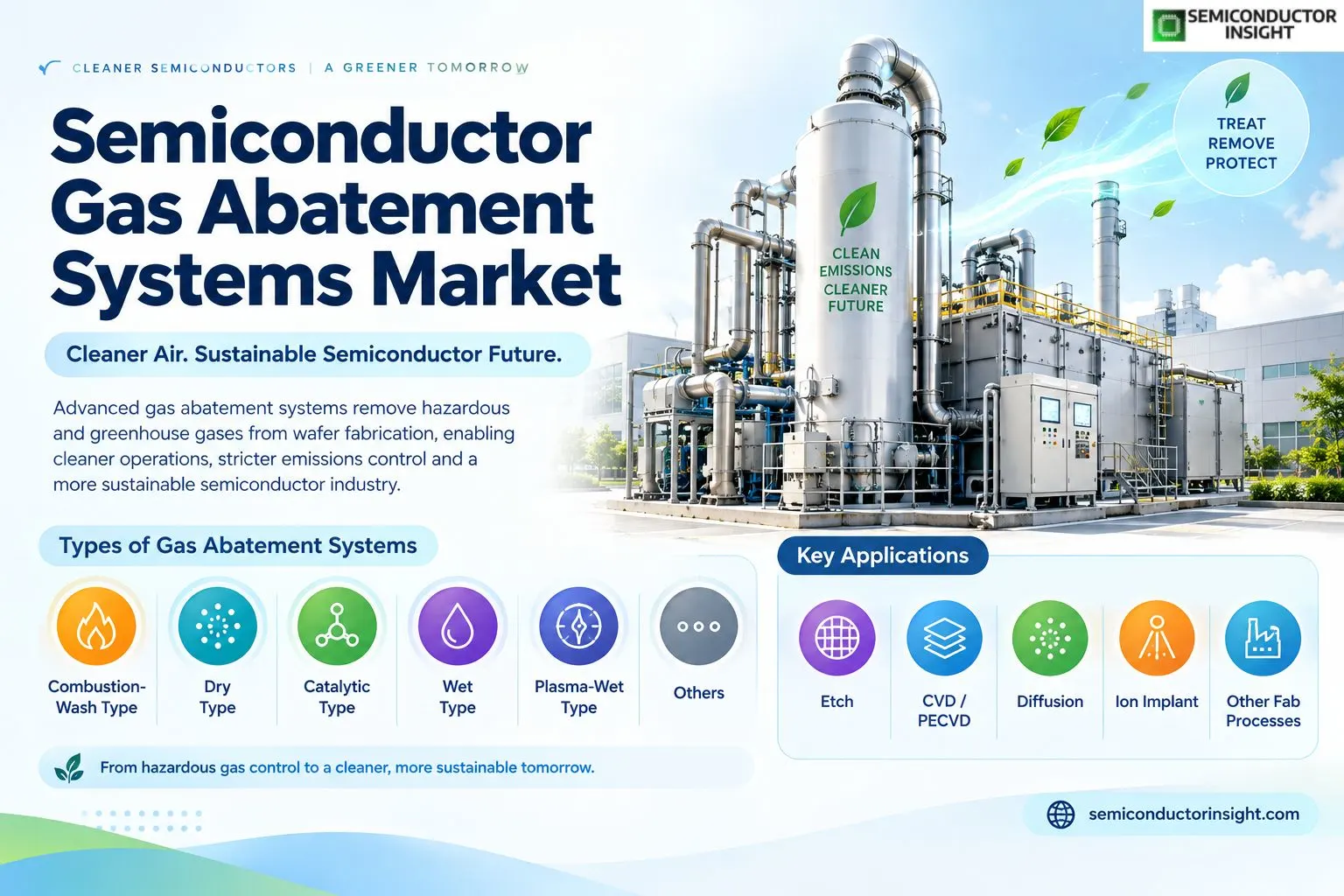
Semiconductor gas abatement systems treat hazardous and greenhouse-gas exhaust from wafer fabrication before discharge, using combustion, plasma, wet scrubbing, dry adsorption or catalytic conversion. Commercial decisions in the Semiconductor Gas Abatement Systems market therefore depend on system integration, qualification effort, reliability, lifecycle support and measurable operating value rather than on one specification alone.
The client evidence values the market at USD 1.383 billion in 2024 and projects USD 2.813 billion by 2032 at a 10.9% CAGR. Expansion of semiconductor fabs and tighter emissions control are the main structural drivers. Supplier selection also reflects manufacturing consistency, regional technical support, product availability and the ability to sustain qualified designs through multi-year customer programs.
Edwards notes that sub-fabs can contain hundreds or thousands of vacuum and abatement systems, and its current semiconductor portfolio combines abatement, vacuum and smart-service tools. Modern systems focus increasingly on energy, water use and predictive maintenance. Buyers increasingly compare total system impact, implementation complexity and long-term service requirements alongside component price, which creates room for technically differentiated suppliers.
Segment Analysis: By Type
By type, the semiconductor gas abatement systems market is segmented into Combustion-Wash Type, Dry Type, Catalytic Type, Wet Type, Plasma-Wet Type, Others. Each category has a distinct functional role and commercial position, so the analysis emphasizes use case, integration and competitive relevance rather than repeating a single market statistic across every row.
| Type | Function | Market position |
|---|---|---|
| Combustion-Wash Type | Combustion-Wash Type addresses a distinct architecture or performance requirement within the Semiconductor Gas Abatement Systems market. | Commercial demand depends on application fit, qualification, cost and lifecycle requirements rather than a single headline statistic. |
| Dry Type | Dry Type addresses a distinct architecture or performance requirement within the Semiconductor Gas Abatement Systems market. | Commercial demand depends on application fit, qualification, cost and lifecycle requirements rather than a single headline statistic. |
| Catalytic Type | Catalytic Type addresses a distinct architecture or performance requirement within the Semiconductor Gas Abatement Systems market. | Commercial demand depends on application fit, qualification, cost and lifecycle requirements rather than a single headline statistic. |
| Wet Type | Wet Type addresses a distinct architecture or performance requirement within the Semiconductor Gas Abatement Systems market. | Commercial demand depends on application fit, qualification, cost and lifecycle requirements rather than a single headline statistic. |
| Plasma-Wet Type | Plasma-Wet Type addresses a distinct architecture or performance requirement within the Semiconductor Gas Abatement Systems market. | Commercial demand depends on application fit, qualification, cost and lifecycle requirements rather than a single headline statistic. |
| Others | Others addresses a distinct architecture or performance requirement within the Semiconductor Gas Abatement Systems market. | Commercial demand depends on application fit, qualification, cost and lifecycle requirements rather than a single headline statistic. |
Pricing by type
Combustion-wash systems carry significant value through gas-treatment versatility, while plasma and catalytic systems command premiums where lower utility use or specific gas chemistries justify the technology. Adoption varies by customer architecture and replacement cycle, so demand is strongest where the technology solves a clear performance, reliability or integration problem. That market structure favors suppliers able to combine product performance with stable supply, application engineering and documented quality across the intended operating environment.
Segment Analysis: By Application
By application, the market is segmented into Etch, CVD / PECVD, Diffusion, Ion Implant, Other Fab Processes. Application economics differ by qualification, lifecycle, reliability and system-level value, so each row below uses context specific to that application rather than mechanically repeating headline evidence. Commercial decisions in the Semiconductor Gas Abatement Systems market therefore depend on system integration, qualification effort, reliability, lifecycle support and measurable operating value rather than on one specification alone.
| Application | Demand characteristics |
|---|---|
| Etch | Etch creates demand where semiconductor gas abatement systems improves integration, performance, reliability or system economics. |
| CVD / PECVD | CVD / PECVD creates demand where semiconductor gas abatement systems improves integration, performance, reliability or system economics. |
| Diffusion | Diffusion creates demand where semiconductor gas abatement systems improves integration, performance, reliability or system economics. |
| Ion Implant | Ion Implant creates demand where semiconductor gas abatement systems improves integration, performance, reliability or system economics. |
| Other Fab Processes | Other Fab Processes creates demand where semiconductor gas abatement systems improves integration, performance, reliability or system economics. |
Regional Analysis
Asia Pacific leads current market value, while Asia Pacific has the strongest growth profile. Regional demand is shaped by manufacturing concentration, technology adoption, customer investment cycles and local supplier ecosystems. Supplier selection also reflects manufacturing consistency, regional technical support, product availability and the ability to sustain qualified designs through multi-year customer programs.
How does regional demand differ across the semiconductor gas abatement systems market?
Asia Pacific provides the deepest manufacturing scale, North America contributes high-value technology and enterprise demand, and Europe remains important in industrial, automotive and regulated applications. South America and the Middle East & Africa are smaller but developing markets. Buyers increasingly compare total system impact, implementation complexity and long-term service requirements alongside component price, which creates room for technically differentiated suppliers.
| Region | Position | Growth outlook | Demand profile | What decides supplier selection |
|---|---|---|---|---|
| Asia Pacific | Largest | Highest | fab expansion in Taiwan, South Korea, China and Southeast Asia | Supply scale and qualification |
| North America | High | Moderate-high | advanced logic fabs, environmental compliance and sub-fab modernization | Technology capability and service |
| Europe | Moderate-high | Moderate | semiconductor manufacturing, sustainability regulation and equipment upgrades | Compliance and lifecycle |
| South America | Smaller | Moderate | Import/industrial led | Cost and distribution |
| Middle East & Africa | Smallest base | Emerging | Infrastructure led | Project support |
Key Semiconductor Gas Abatement Systems Manufacturers and Competitive Landscape
The competitive landscape includes Ebara, Edwards Vacuum, GST, Busch Vacuum Solutions, CS Clean Solutions, DAS Environmental Expert, Ecosys, Centrotherm, Critical Systems, SCREEN/related suppliers. Buyers increasingly compare total system impact, implementation complexity and long-term service requirements alongside component price, which creates room for technically differentiated suppliers. Adoption varies by customer architecture and replacement cycle, so demand is strongest where the technology solves a clear performance, reliability or integration problem.
Competition centers on higher destruction efficiency, lower fuel/water consumption and predictive maintenance, customer qualification, manufacturing consistency and application support. Once a product is designed into a long-lifecycle system, switching costs can protect incumbent positions but also raise the importance of roadmap continuity. That market structure favors suppliers able to combine product performance with stable supply, application engineering and documented quality across the intended operating environment.
Tier structure
| Tier | Companies | Basis of competition |
|---|---|---|
| Tier 1 | Ebara, Edwards Vacuum, GST, Busch Vacuum Solutions | Global scale, broad customer qualification and advanced technology portfolios. |
| Tier 2 | CS Clean Solutions, DAS Environmental Expert, Ecosys, Centrotherm | Strong specialist capability, regional design wins and application-focused portfolios. |
| Tier 3 | Regional and niche suppliers | Cost competition, customization and specialized customer support. |
Key companies profiled
- Ebara
- Edwards Vacuum
- GST
- Busch Vacuum Solutions
- CS Clean Solutions
- DAS Environmental Expert
- Ecosys
- Centrotherm
- Critical Systems
- SCREEN/related suppliers
Semiconductor Gas Abatement Systems Production Capacity Analysis
Production capacity in the Semiconductor Gas Abatement Systems market is shaped by the underlying manufacturing process, qualification burden and customer-specific configuration. Suppliers must balance equipment utilization with quality control because high-volume output only creates value when yield, reliability and traceability remain stable. Commercial decisions in the Semiconductor Gas Abatement Systems market therefore depend on system integration, qualification effort, reliability, lifecycle support and measurable operating value rather than on one specification alone.
Capacity additions tend to follow customer program ramps rather than headline market growth alone. Regional supply resilience is becoming more important, particularly where customers require second-source planning, long product lifecycles or shorter engineering-response times. Supplier selection also reflects manufacturing consistency, regional technical support, product availability and the ability to sustain qualified designs through multi-year customer programs.
The practical bottleneck is often qualified output rather than nominal installed capacity. Manufacturing, assembly, test and application support must scale together to avoid creating capacity that cannot be used in production programs. Buyers increasingly compare total system impact, implementation complexity and long-term service requirements alongside component price, which creates room for technically differentiated suppliers.
Semiconductor Gas Abatement Systems Market Dynamics: Drivers, Restraints and Opportunities
The Semiconductor Gas Abatement Systems market is shaped by growth is driven by new fabs, advanced-node process intensity, emissions regulation and wider use of nf3, pfcs, hydrides and other gases requiring specialized point-of-use treatment. At the same time, growth is constrained by high capital and utility cost, process-specific gas chemistry, maintenance burden, footprint and the need to validate destruction efficiency without affecting process uptime. The strongest commercial opportunities are concentrated in smart abatement, lower-carbon systems, resource recovery and integrated pump-abatement platforms create the strongest opportunities.
MARKET DRIVERS
Drivers Impact Analysis*
| Driver | (~) % impact on CAGR forecast | Geographic relevance | Impact timeline |
|---|---|---|---|
| Technology upgrade cycle | +1.6% | Global; strongest in leading adopter markets | Near to medium term |
| End-market expansion | +1.2% | Application-specific | Near term |
| Higher value per system | +0.8% | Premium and advanced systems | Medium term |
Technology adoption expands addressable demand
Growth is driven by new fabs, advanced-node process intensity, emissions regulation and wider use of NF3, PFCs, hydrides and other gases requiring specialized point-of-use treatment. This demand is strongest where customers can measure a clear improvement in system performance, footprint, energy efficiency, reliability or operating cost. Adoption varies by customer architecture and replacement cycle, so demand is strongest where the technology solves a clear performance, reliability or integration problem.
End-market modernization increases content per system
The technology upgrade cycle supports replacement and redesign activity as OEMs move to higher-performance architectures. New designs typically create the best opportunity because suppliers can influence specifications before qualification is locked. That market structure favors suppliers able to combine product performance with stable supply, application engineering and documented quality across the intended operating environment.
Higher-value architectures support premium mix
Expanding end markets also increase content per system, creating value growth even when unit shipments grow more slowly. Suppliers that combine engineering support with reliable supply are better positioned to capture those design transitions. Commercial decisions in the Semiconductor Gas Abatement Systems market therefore depend on system integration, qualification effort, reliability, lifecycle support and measurable operating value rather than on one specification alone.
MARKET RESTRAINTS
Restraints Impact Analysis*
| Restraint | (~) % impact on CAGR forecast | Geographic relevance | Impact timeline |
|---|---|---|---|
| Qualification and integration burden | -0.7% | Global | Ongoing |
| Price and substitution pressure | -0.5% | Cost-sensitive applications | Ongoing |
| Supply-chain or process complexity | -0.4% | Global | Medium term |
Qualification burden slows supplier switching
Growth is constrained by high capital and utility cost, process-specific gas chemistry, maintenance burden, footprint and the need to validate destruction efficiency without affecting process uptime. These constraints are most significant where customers have qualified alternatives or where the technology must prove a clear system-level advantage over lower-cost incumbent solutions.
Price competition limits margin expansion
Qualification and integration can extend sales cycles because customers must validate performance, reliability and compatibility in their own system environment. That makes early engineering engagement important for new suppliers. Supplier selection also reflects manufacturing consistency, regional technical support, product availability and the ability to sustain qualified designs through multi-year customer programs.
Alternative technologies constrain selected use cases
Supply-chain complexity can also limit growth when specialized materials, tooling, test or regional support are required. Customers increasingly evaluate resilience alongside price when choosing long-lifecycle suppliers. Buyers increasingly compare total system impact, implementation complexity and long-term service requirements alongside component price, which creates room for technically differentiated suppliers. Adoption varies by customer architecture and replacement cycle, so demand is strongest where the technology solves a clear performance, reliability or integration problem.
MARKET OPPORTUNITIES
Advanced integration creates premium opportunities
Smart abatement, lower-carbon systems, resource recovery and integrated pump-abatement platforms create the strongest opportunities. The most attractive opportunities are where customers are redesigning systems rather than simply replacing like-for-like components. That market structure favors suppliers able to combine product performance with stable supply, application engineering and documented quality across the intended operating environment.
Regional capacity and supply resilience
Higher destruction efficiency, lower fuel/water consumption and predictive maintenance can create premium value when it lowers system complexity, improves performance or supports a new product architecture that is difficult to achieve with incumbent approaches. Commercial decisions in the Semiconductor Gas Abatement Systems market therefore depend on system integration, qualification effort, reliability, lifecycle support and measurable operating value rather than on one specification alone.
Application engineering deepens customer value
Regional engineering support and application-specific customization provide another route to growth because customers increasingly expect suppliers to support qualification, transition planning and lifecycle management. Supplier selection also reflects manufacturing consistency, regional technical support, product availability and the ability to sustain qualified designs through multi-year customer programs. Buyers increasingly compare total system impact, implementation complexity and long-term service requirements alongside component price, which creates room for technically differentiated suppliers.
Semiconductor Gas Abatement Systems Supply Chain Analysis
Upstream. Combustion chambers, plasma sources, scrubbers, catalysts, sensors, pumps, gas monitoring, water systems and digital service software form the supply chain. Supply quality at this stage directly affects downstream yield, reliability and cost. Adoption varies by customer architecture and replacement cycle, so demand is strongest where the technology solves a clear performance, reliability or integration problem.
Manufacturing. Core production combines process control, assembly, inspection and test, with product-specific qualification used to verify performance before customer shipment. That market structure favors suppliers able to combine product performance with stable supply, application engineering and documented quality across the intended operating environment. Commercial decisions in the Semiconductor Gas Abatement Systems market therefore depend on system integration, qualification effort, reliability, lifecycle support and measurable operating value rather than on one specification alone.
Distribution. High-value programs are typically won through direct OEM, Tier-1 or design-house engagement, while distributors serve prototypes, regional customers and lower-volume applications. Supplier selection also reflects manufacturing consistency, regional technical support, product availability and the ability to sustain qualified designs through multi-year customer programs. Buyers increasingly compare total system impact, implementation complexity and long-term service requirements alongside component price, which creates room for technically differentiated suppliers.
Downstream. End users integrate the product into systems where switching costs rise after qualification, making lifecycle support and supply continuity commercially important. Adoption varies by customer architecture and replacement cycle, so demand is strongest where the technology solves a clear performance, reliability or integration problem. That market structure favors suppliers able to combine product performance with stable supply, application engineering and documented quality across the intended operating environment.
Downstream. Panel builders and machine OEMs are the primary specifying customers, followed by electrical contractors working on building services and by facility maintenance teams handling replacement. The specification decision is usually made once, at panel design, and then repeats for the life of the design — which makes design-in position considerably more valuable than any individual transaction.
Recent Developments in the Semiconductor Gas Abatement Systems Market
Developments tracked through September 2026. Items are selected for direct relevance to product technology, deployment or standards. Commercial decisions in the Semiconductor Gas Abatement Systems market therefore depend on system integration, qualification effort, reliability, lifecycle support and measurable operating value rather than on one specification alone. Supplier selection also reflects manufacturing consistency, regional technical support, product availability and the ability to sustain qualified designs through multi-year customer programs.
- 2026 Current
Edwards focuses on smart sub-fab performance Edwards continues integrating vacuum and abatement with data-driven monitoring to improve fab uptime and process stability. Source - 2026 Industry Event
SEMI ESGS 2026 includes abatement sustainability update The 2026 Electronic Specialty Gases & Systems Conference includes semiconductor abatement, emissions monitoring and sustainability sessions. Source - 2026 Current
Edwards semiconductor abatement portfolio Edwards continues offering environmental abatement products alongside dry pumps and integrated sub-fab systems. Source
REPORT SCOPE & SEGMENTATION
| Attribute | Details |
|---|---|
| Study Period | 2021–2034 |
| Base Year | 2025 |
| Estimated Year | 2026 |
| Forecast Period | 2026–2034 |
| Historical Period | 2021–2025 |
| Market Size 2025 | USD 1.53 billion |
| Market Size 2034 | USD 3.89 billion |
| Growth Rate | CAGR of 10.9% from 2026–2034 |
| Unit | Value (USD Million) |
| Segmentation | By Type, By Application, By Installation, By Gas Family, and By Region |
| By Type | Combustion-Wash Type · Dry Type · Catalytic Type · Wet Type · Plasma-Wet Type · Others |
| By Application | Etch · CVD / PECVD · Diffusion · Ion Implant · Other Fab Processes |
| By Gas Family | PFC / NF3 / SF6 · Hydrides · Dopants · VOC / Other |
| By Installation | Point-of-Use · Centralized |
| By Region | Each region analysed by Type, Application and Country North AmericaU.S., Canada, Mexico EuropeGermany, France, U.K., Italy, Russia, Nordic Countries, Benelux AsiaChina, Japan, South Korea, India, Southeast Asia South AmericaBrazil, Argentina, Rest of South America Middle East & AfricaTurkey, Israel, Saudi Arabia, UAE, Rest of MEA |
| Key Companies Profiled | Ebara, Edwards Vacuum, GST, Busch Vacuum Solutions, CS Clean Solutions, DAS Environmental Expert, Ecosys, Centrotherm, Critical Systems, SCREEN/related suppliers |
| Customization Scope | Free report customization (equivalent to up to 4 analyst working days) with purchase. Addition or alteration to country, regional and segment scope. |
Frequently Asked Questions
What is the current size of the Semiconductor Gas Abatement Systems market?
The market is valued at USD 1.53 billion in 2025 and is projected to reach USD 3.89 billion by 2034, expanding at a 10.9% CAGR during 2026–2034.
Which companies lead the Semiconductor Gas Abatement Systems market?
Key participants include Ebara, Edwards Vacuum, GST, Busch Vacuum Solutions, CS Clean Solutions, DAS Environmental Expert, Ecosys, Centrotherm.
What is Semiconductor Gas Abatement Systems?
Semiconductor gas abatement systems treat hazardous and greenhouse-gas exhaust from wafer fabrication before discharge, using combustion, plasma, wet scrubbing, dry adsorption or catalytic conversion.
What are the main product types?
The market includes Combustion-Wash Type, Dry Type, Catalytic Type, Wet Type, Plasma-Wet Type, Others.
What are the key applications?
The principal applications are Etch, CVD / PECVD, Diffusion, Ion Implant, Other Fab Processes.
Which region leads the market?
Asia Pacific leads current market value, while Asia Pacific has the strongest growth profile.
What drives market growth?
Growth is driven by new fabs, advanced-node process intensity, emissions regulation and wider use of NF3, PFCs, hydrides and other gases requiring specialized point-of-use treatment.
What are the main challenges?
Growth is constrained by high capital and utility cost, process-specific gas chemistry, maintenance burden, footprint and the need to validate destruction efficiency without affecting process uptime.
Research Sources & Evidence Base
Get Sample Report PDF for Exclusive Insights
Report Sample Includes
- Table of Contents
- List of Tables & Figures
- Charts, Research Methodology, and more...
 Download Sample Report PDF

