MARKET INSIGHTS
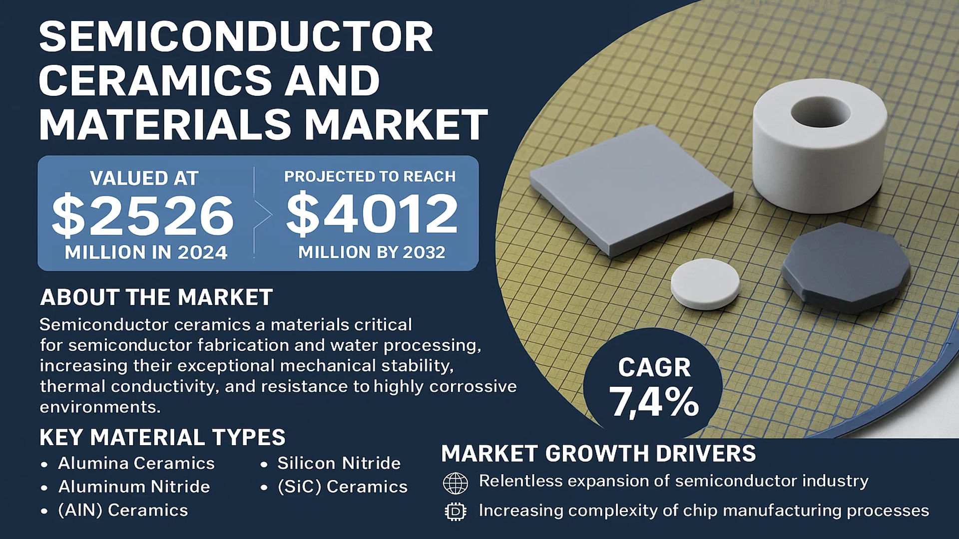
The global Semiconductor Ceramics and Materials Market was valued at 2526 million in 2024 and is projected to reach US$ 4012 million by 2032, at a CAGR of 7.4% during the forecast period.
Semiconductor ceramics and materials are a class of engineered technical ceramics critical for semiconductor fabrication and wafer processing. These materials are prized for their exceptional mechanical stability, thermal conductivity, and resistance to highly corrosive environments. They are integral components in a wide array of semiconductor manufacturing equipment, including systems for Chemical Vapor Deposition (CVD), etching, ion implantation, lithography, and wafer handling. Key material types include Alumina Ceramics, Aluminum Nitride (AlN) Ceramics, Silicon Carbide (SiC) Ceramics, and Silicon Nitride (Si3N4) Ceramics.
The market growth is primarily driven by the relentless expansion of the global semiconductor industry and the increasing complexity of chip manufacturing processes. The push towards advanced packaging and heterogeneous integration further amplifies the demand for high-performance ceramic components that ensure hermeticity and thermal management. Geographically, the market is highly concentrated, with manufacturers from Japan holding a dominant share of approximately 68%, followed by players from the United States and Europe. Recent strategic expansions and acquisitions by key players like NGK Insulators, Kyocera, and Coorstek are consolidating the market and strengthening their positions to cater to the next generation of semiconductor manufacturing needs.
MARKET DYNAMICS
MARKET DRIVERS
Expansion of Semiconductor Fabrication Facilities Globally to Drive Market Growth
The global semiconductor industry is witnessing unprecedented expansion driven by increasing demand for advanced electronics, artificial intelligence, and high-performance computing. This expansion necessitates significant investment in fabrication facilities, which directly fuels demand for semiconductor ceramics and materials. These materials are essential components in wafer processing equipment, including deposition systems, etch tools, and thermal processing chambers. The ongoing construction of new fabrication plants worldwide represents a substantial growth driver, with investment in semiconductor manufacturing equipment reaching record levels in recent years. This sustained capital expenditure ensures continuous demand for high-performance ceramic components that can withstand extreme processing conditions while maintaining dimensional stability and purity requirements.
Advancements in Semiconductor Manufacturing Technologies to Boost Material Requirements
Technological evolution in semiconductor manufacturing, particularly the transition to smaller process nodes and three-dimensional architectures, is creating increased demand for advanced ceramic materials. As feature sizes shrink below 5 nanometers, manufacturing processes require materials with exceptional thermal stability, minimal particle generation, and superior chemical resistance. Ceramics such as aluminum nitride and silicon carbide provide critical performance advantages in these advanced applications, enabling higher processing temperatures and improved process control. The shift toward more complex device structures has correspondingly increased the sophistication of ceramic components used in processing equipment, driving both volume growth and value enhancement within the market.
Furthermore, the integration of new materials in semiconductor manufacturing, including gallium nitride and silicon carbide power devices, creates additional opportunities for specialized ceramic substrates and components.
➤ For instance, the growing adoption of wide-bandgap semiconductors in power electronics and electric vehicles requires ceramic materials with enhanced thermal management properties, driving innovation and market expansion.
Additionally, the increasing complexity of semiconductor manufacturing equipment, with higher chamber temperatures and more aggressive process chemistries, continues to push the performance requirements for ceramic components, supporting market growth through technological advancement.
MARKET CHALLENGES
High Manufacturing Costs and Technical Complexity to Challenge Market Participants
The semiconductor ceramics market faces significant challenges related to the high costs and technical complexity of manufacturing advanced ceramic components. Producing ceramics that meet the stringent purity, dimensional stability, and performance requirements of semiconductor applications requires substantial capital investment in specialized equipment and facilities. The manufacturing processes involve multiple sophisticated steps including powder preparation, forming, sintering, and precision machining, each requiring tight control and extensive quality assurance measures. These factors contribute to high production costs that can challenge market accessibility, particularly for smaller manufacturers and emerging market participants.
Other Challenges
Stringent Quality and Performance Requirements
Semiconductor manufacturers impose exceptionally rigorous quality standards on ceramic components, requiring near-perfect material properties and minimal defect rates. Components must demonstrate exceptional purity levels, typically with metallic contamination below single-digit parts per million, while maintaining precise dimensional tolerances often measured in micrometers. Meeting these requirements consistently presents ongoing challenges for material suppliers and adds considerable complexity to manufacturing processes and quality control systems.
Rapid Technological Obsolescence
The fast pace of semiconductor technology development creates challenges related to product lifecycle management and technological obsolescence. Ceramic components developed for specific equipment generations may become obsolete within relatively short timeframes as manufacturing technologies advance, requiring continuous research and development investment to maintain market relevance. This dynamic environment demands significant resources for staying current with evolving customer requirements and technology trends.
MARKET RESTRAINTS
Supply Chain Vulnerabilities and Material Sourcing Constraints to Limit Market Growth
The semiconductor ceramics market faces significant restraints from supply chain vulnerabilities and constraints in raw material sourcing. Many advanced ceramic materials require high-purity raw materials that are subject to supply chain disruptions and price volatility. Certain critical raw materials, including specialized alumina powders and high-purity silicon carbide precursors, face supply constraints due to limited global production capacity and geopolitical factors. These challenges are compounded by the concentrated nature of the semiconductor equipment market, where demand fluctuations can create significant supply-demand imbalances.
Additionally, the specialized nature of ceramic component manufacturing creates lengthy qualification processes that can restrain market responsiveness to changing demand patterns. The time required to qualify new suppliers and establish reliable production capacity often extends to multiple quarters, creating barriers to rapid market expansion during periods of increased demand.
MARKET OPPORTUNITIES
Emerging Applications in Advanced Packaging and Heterogeneous Integration to Create Growth Opportunities
The evolution of semiconductor packaging technologies presents significant growth opportunities for advanced ceramic materials. As the industry moves toward advanced packaging approaches including 2.5D and 3D integration, fan-out wafer-level packaging, and system-in-package solutions, new requirements emerge for ceramic substrates and components. These applications demand materials with enhanced thermal management capabilities, improved coefficient of thermal expansion matching, and superior electrical properties. The growing adoption of heterogeneous integration, where multiple die types are combined in single packages, particularly drives demand for specialized ceramic materials that can address the complex thermal and mechanical challenges involved.
Furthermore, the expansion of semiconductor applications into automotive, industrial, and aerospace sectors creates additional opportunities for ceramic materials capable of operating in harsh environments and extended temperature ranges. These applications often require ceramics with enhanced reliability and longevity, supporting market diversification beyond traditional semiconductor manufacturing equipment.
SEMICONDUCTOR CERAMICS AND MATERIALS MARKET TRENDS
Miniaturization and Advanced Node Fabrication Driving Material Innovation
The relentless push towards semiconductor miniaturization, particularly below the 5nm node, has emerged as a primary catalyst for innovation within the semiconductor ceramics and materials market. This trend demands components with exceptional thermal management, superior electrical insulation, and extreme mechanical stability under highly corrosive process conditions. Consequently, there is a significant shift towards high-purity aluminum nitride (AlN) ceramics, which offer thermal conductivity exceeding 170 W/mK, and silicon carbide (SiC) for applications requiring extreme hardness and chemical inertness. The transition to more complex 3D chip architectures, such as FinFETs and Gate-All-Around (GAA) transistors, further intensifies the need for specialized ceramic components in wafer handling, electrostatic chucks (ESCs), and plasma-resistant chamber liners. This evolution is fundamentally reshaping material requirements, as traditional alumina compositions are increasingly being supplemented or replaced by advanced formulations to meet the stringent demands of next-generation lithography, etch, and deposition equipment.
Other Trends
Geopolitical Reshoring and Supply Chain Diversification
Geopolitical tensions and a heightened focus on supply chain security are profoundly influencing market dynamics, prompting a strategic shift in manufacturing and sourcing. Initiatives like the CHIPS and Science Act in the United States, which allocates over $52 billion in funding, are accelerating domestic investment in semiconductor fabrication facilities. This creates parallel demand for a localized and resilient supply chain for critical ceramic components. Similarly, Japan and South Korea are reinforcing their dominant positions through government-backed initiatives, with Japanese manufacturers currently holding approximately 68% of the global market share. This trend is not merely about building new fabs but also about securing the entire material ecosystem, leading to increased partnerships, joint ventures, and capacity expansions by key ceramic material suppliers to ensure they can support the geographically dispersed production base of their semiconductor manufacturing equipment (SME) customers.
Sustainability and Process Efficiency Gains
A growing emphasis on operational sustainability and cost reduction within semiconductor fabs is driving the adoption of ceramics designed for enhanced longevity and process efficiency. The extreme environments inside etch and CVD chambers cause significant wear on components, leading to costly downtime for replacement and maintenance. In response, material scientists are developing new ceramic coatings and bulk materials with vastly improved erosion and corrosion resistance, directly contributing to longer mean time between failures (MTBF) and reduced particle contamination. For instance, advancements in yttria-based coatings are proving highly effective in mitigating plasma erosion. Furthermore, the integration of Internet of Things (IoT) sensors directly into ceramic components is an emerging trend, enabling real-time monitoring of part health and process conditions. This allows for predictive maintenance, optimizing consumable life and significantly improving overall equipment effectiveness (OEE), which is a critical metric for high-volume manufacturing facilities.
COMPETITIVE LANDSCAPE
Key Industry Players
Companies Strive to Strengthen their Product Portfolio to Sustain Competition
The global semiconductor ceramics and materials market exhibits a highly concentrated competitive structure, dominated by a handful of established players who command a significant majority of the market share. This concentration is primarily due to the high technical barriers to entry, including the need for advanced material science expertise, stringent purity requirements, and deep integration with semiconductor fabrication equipment manufacturers. The market is characterized by intense competition based on product performance, reliability, and the ability to meet the evolving demands of next-generation chip manufacturing processes.
NGK Insulators and Kyocera Corporation are unequivocally the market leaders, a position solidified by their extensive portfolios and long-standing relationships with major semiconductor capital equipment OEMs. Their dominance is further underscored by the fact that Japanese manufacturers collectively hold approximately 68% of the global market share, reflecting the country’s historical strength in advanced ceramics. These giants leverage their scale to invest heavily in research and development, focusing on materials for extreme environments encountered in etching, deposition, and thermal processing.
Following closely, Ferrotec, TOTO Advanced Ceramics, and Morgan Advanced Materials also hold substantial market positions. Their growth is intrinsically linked to their innovative material solutions, particularly in Aluminum Nitride (AlN) and Silicon Carbide (SiC) ceramics, which are critical for applications requiring superior thermal management. These companies are actively pursuing geographical expansions and strategic acquisitions to bolster their production capabilities and enhance their global supply chain resilience, which is paramount for serving the geographically dispersed semiconductor industry.
Meanwhile, Western players like Coorstek and 3M are strengthening their market presence through significant investments in proprietary technologies and custom-engineered solutions. Their strategy often involves focusing on high-value, specialized components for specific tool types, allowing them to compete effectively despite the overall market share dominance of Japanese firms. Furthermore, regional players in South Korea and China, such as MiCo Ceramics and WONIK QnC, are growing rapidly, supported by strong domestic semiconductor industries and government initiatives aimed at supply chain localization.
List of Key Semiconductor Ceramics and Materials Companies Profiled
- NGK Insulators Ltd. (Japan)
- Kyocera Corporation (Japan)
- Ferrotec Corporation (Japan)
- TOTO Advanced Ceramics (Japan)
- Morgan Advanced Materials (U.K.)
- Coorstek, Inc. (U.S.)
- 3M Company (U.S.)
- Niterra Co., Ltd. (Japan)
- ASUZAC Fine Ceramics (Japan)
Segment Analysis:
By Type
Alumina Ceramics Segment Dominates the Market Due to its Excellent Mechanical Stability and Cost-Effectiveness
The market is segmented based on type into:
- Alumina Ceramics
- AlN Ceramics
- SiC Ceramics
- Si3N4 Ceramics
- Others
By Application
Semiconductor Deposition Equipment Segment Leads Due to Critical Role in Thin Film Fabrication Processes
The market is segmented based on application into:
- Semiconductor Deposition Equipment
- Semiconductor Etch Equipment
- Lithography Machines
- Ion Implant Equipment
- Heat Treatment Equipment
- CMP Equipment
- Wafer Handling
- Assembly Equipment
- Others
By Region
Asia-Pacific Region Commands the Market Driven by its Dominant Semiconductor Manufacturing Ecosystem
The market is segmented based on region into:
- North America
- Europe
- Asia-Pacific
- South America
- Middle East & Africa
By End-User
Integrated Device Manufacturers (IDMs) Represent a Key Segment Due to High Volume Consumption
The market is segmented based on end-user into:
- Integrated Device Manufacturers (IDMs)
- Foundries
- Semiconductor Equipment OEMs
- Research & Development Institutes
Regional Analysis: Semiconductor Ceramics and Materials Market
Asia-Pacific
Asia-Pacific is the undisputed leader in the global semiconductor ceramics and materials market, commanding the largest production share and consumption volume. This dominance is primarily driven by Japan, which holds an estimated 68% of the global manufacturing share, followed by significant contributions from South Korea, Taiwan, and China. The region is the epicenter of global semiconductor fabrication, housing the world’s leading foundries and memory chip manufacturers. This massive concentration of front-end semiconductor manufacturing facilities creates immense, sustained demand for high-performance ceramic components used in wafer processing equipment. Key applications include critical parts for etch equipment, deposition systems (CVD, PVD, ALD), and lithography machines. While Japan’s established giants like NGK Insulators, Kyocera, and TOTO Advanced Ceramics lead in technological innovation and supply, China is aggressively expanding its domestic capabilities through substantial government-backed investments, aiming to achieve self-sufficiency in the semiconductor supply chain. This strategic push is fostering the growth of local material suppliers and creating a dynamic, highly competitive landscape.
North America
North America represents a vital innovation and advanced manufacturing hub for semiconductor ceramics, characterized by a strong focus on research, development, and high-value specialty products. The region’s market is propelled by the presence of major semiconductor equipment OEMs and the strategic push to onshore critical parts of the chipmaking supply chain, supported by initiatives like the U.S. CHIPS and Science Act. American players, holding approximately 10.2% of the global market, such as Coorstek and 3M, are renowned for their expertise in advanced materials like high-purity Alumina and Aluminum Nitride (AlN) ceramics, which are essential for their superior thermal management properties in demanding applications. The demand is closely tied to the development and manufacturing of cutting-edge semiconductor fabrication tools, including tools for ion implant, advanced lithography, and wafer inspection. Collaboration between national laboratories, academic institutions, and private companies is a key driver, fostering innovation in next-generation ceramic materials needed for future process nodes beyond 3nm.
Europe
The European market for semiconductor ceramics and materials is a significant and technologically advanced region, accounting for roughly 10.3% of global production. It is characterized by a strong presence of specialized manufacturers that focus on high-precision, high-reliability components. European companies like Morgan Advanced Materials and CeramTec are recognized for their deep materials science expertise and ability to produce highly engineered ceramic solutions that meet stringent quality and performance specifications. The market benefits from the region’s robust automotive and industrial sectors, which demand semiconductors manufactured using reliable and durable equipment components. Key applications driving demand include ceramics for heat treatment furnaces, diffusion systems, and wafer handling components within fabrication plants. Furthermore, European environmental and safety regulations influence material development, pushing for sustainable and safe manufacturing processes for these advanced ceramics. The region’s growth is steady, underpinned by continuous innovation and its role as a supplier to global semiconductor capital equipment leaders.
South America
The semiconductor ceramics and materials market in South America is currently nascent and represents a minor segment of the global landscape. The region does not host significant front-end semiconductor fabrication facilities, which are the primary consumers of these advanced materials. Consequently, demand is largely limited to downstream applications, maintenance, and replacement parts for existing industrial and electronics manufacturing equipment. Economic volatility and a lack of substantial local investment in semiconductor manufacturing infrastructure have historically hindered the development of a native market for these specialized materials. Any demand is typically met through imports from established global suppliers in Asia, North America, and Europe. While some countries may have small-scale operations in ceramics production for other industries, the specific technological and purity requirements for semiconductor-grade materials place this market outside their current capabilities. Long-term growth is contingent on major, region-wide economic shifts and strategic investments into high-tech manufacturing sectors.
Middle East & Africa
Similar to South America, the Middle East & Africa region is an emerging and very small player in the global semiconductor ceramics market. The market is primarily import-dependent, with demand stemming from the maintenance and operation of electronics assembly and other industrial facilities rather than from core semiconductor fabrication. Certain nations in the Middle East, driven by economic diversification plans like Saudi Arabia’s Vision 2030, are making initial investments into technology and manufacturing sectors. This could potentially create a future, albeit small, niche demand for these materials. However, the absence of a foundational semiconductor fabrication ecosystem, coupled with challenges related to technical expertise and supply chain development, significantly limits market growth in the short to medium term. The region’s focus remains on building basic technological infrastructure, making the market for highly specialized semiconductor ceramics a long-term prospect rather than a current reality.
Report Scope
This market research report provides a comprehensive analysis of the global and regional Semiconductor Ceramics and Materials markets, covering the forecast period 2025–2032. It offers detailed insights into market dynamics, technological advancements, competitive landscape, and key trends shaping the industry.
Key focus areas of the report include:
- Market Size & Forecast: Historical data and future projections for revenue, unit shipments, and market value across major regions and segments.
- Segmentation Analysis: Detailed breakdown by product type, technology, application, and end-user industry to identify high-growth segments and investment opportunities.
- Regional Outlook: Insights into market performance across North America, Europe, Asia-Pacific, Latin America, and the Middle East & Africa, including country-level analysis where relevant.
- Competitive Landscape: Profiles of leading market participants, including their product offerings, R&D focus, manufacturing capacity, pricing strategies, and recent developments such as mergers, acquisitions, and partnerships.
- Technology Trends & Innovation: Assessment of emerging technologies, integration of AI/IoT, semiconductor design trends, fabrication techniques, and evolving industry standards.
- Market Drivers & Restraints: Evaluation of factors driving market growth along with challenges, supply chain constraints, regulatory issues, and market-entry barriers.
- Stakeholder Analysis: Insights for component suppliers, OEMs, system integrators, investors, and policymakers regarding the evolving ecosystem and strategic opportunities.
Primary and secondary research methods are employed, including interviews with industry experts, data from verified sources, and real-time market intelligence to ensure the accuracy and reliability of the insights presented.
FREQUENTLY ASKED QUESTIONS:
What is the current market size of Global Semiconductor Ceramics and Materials Market?
-> Semiconductor Ceramics and Materials Market was valued at 2526 million in 2024 and is projected to reach US$ 4012 million by 2032, at a CAGR of 7.4% during the forecast period.
Which key companies operate in Global Semiconductor Ceramics and Materials Market?
-> Key players include NGK Insulators, Kyocera, Ferrotec, TOTO Advanced Ceramics, Coorstek, Morgan Advanced Materials, Niterra Co., Ltd., ASUZAC Fine Ceramics, and 3M, among others. The top nine players collectively hold over 88% of the global market share.
What are the key growth drivers?
-> Key growth drivers include rising semiconductor fabrication activities, increasing demand for advanced packaging solutions, expansion of AI and IoT applications, and the critical need for materials with high thermal conductivity and environmental stability in corrosive manufacturing environments.
Which region dominates the market?
-> Asia-Pacific is the dominant region, with Japan alone accounting for approximately 68% of global manufacturing share. The region is followed by North America (10.2%) and Europe (10.3%), with significant contributions from South Korea (5.87%).
What are the emerging trends?
-> Emerging trends include development of ultra-high purity ceramics, integration of ceramics in advanced lithography and etching equipment, adoption of silicon nitride and silicon carbide for extreme thermal management, and strategic acquisitions by major players to expand manufacturing capacity and technological portfolios.

Get Sample Report PDF for Exclusive Insights
Report Sample Includes
- Table of Contents
- List of Tables & Figures
- Charts, Research Methodology, and more...


