
Key Statistics
Key Takeaways
- Combustion-type abatement holds the largest share of installed systems in 2025, because thermal destruction remains the qualified default for the pyrophoric and hydride-bearing exhaust streams that dominate deposition and diffusion process steps.
- Catalytic and plasma-assisted systems are the fastest-growing types, selected where destruction efficiency on stable fluorinated compounds is measured and reported rather than merely permitted, and where the energy cost of thermal destruction has become a specification constraint in its own right.
- Foundries are the faster-growing end-user segment while IDMs remain the larger installed base, reflecting the concentration of new leading-edge capacity in foundry hands and the etch-intensive process flows that advanced logic and memory nodes require.
- Asia-Pacific is the largest and fastest-growing region. Abatement is procured per process tool and installed in the sub-fab, so demand sits wherever wafer capacity sits – overwhelmingly Taiwan, South Korea, China and Japan. Europe’s significance is supply-side: it hosts Edwards, DAS Environmental, Busch and CS Clean Solutions.
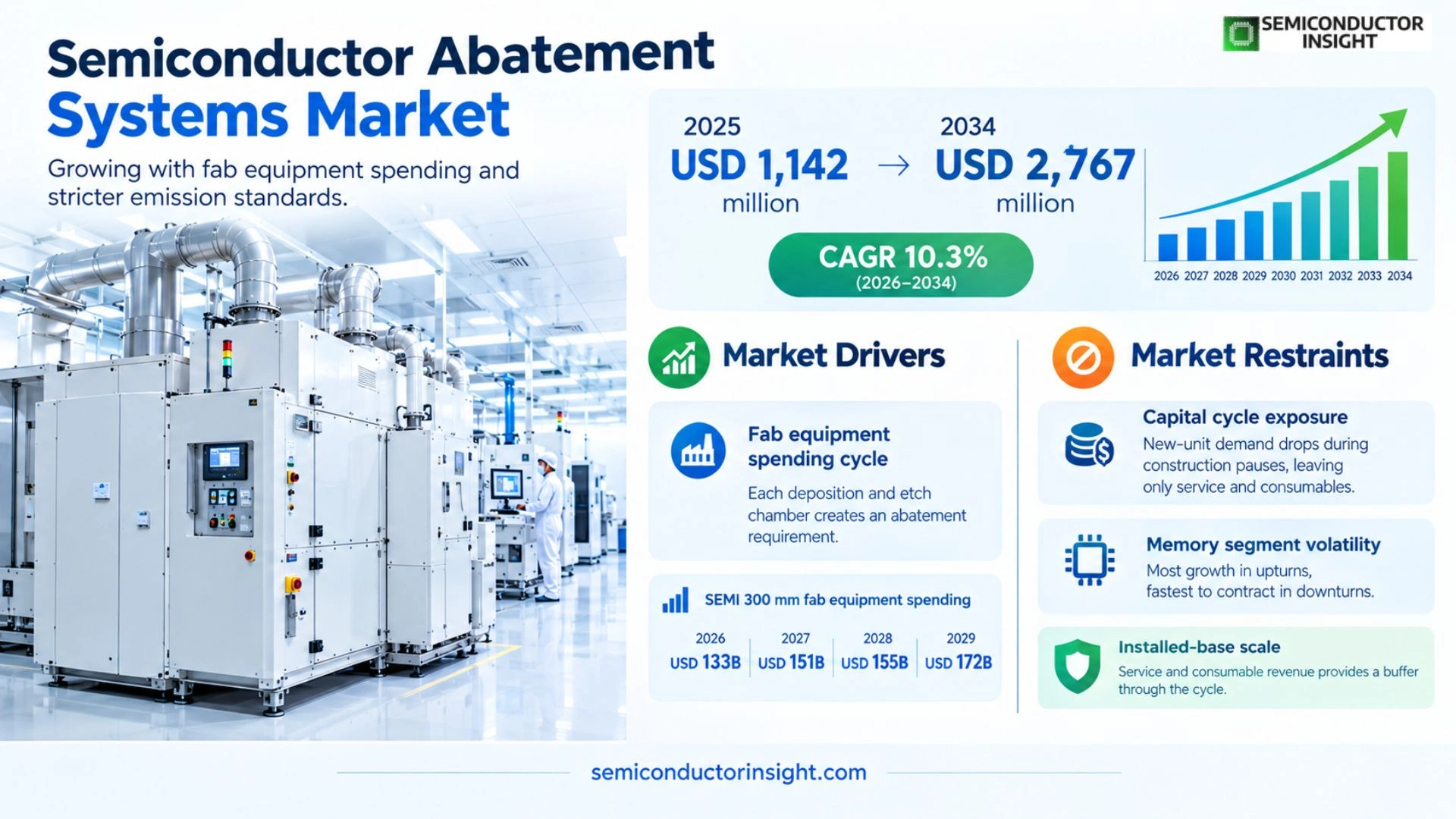
- The market is geared directly to capital equipment spending. SEMI projects 300 mm fab equipment spending of USD 133 billion in 2026, USD 151 billion in 2027 and USD 172 billion in 2029, with cumulative 2027–2029 spending of USD 374 billion – the installation schedule this market is bought against.
- Vacuum and abatement are converging commercially. Edwards, Atlas Copco’s CSK and Busch all sell abatement alongside dry pumps into the same sub-fab, and Atlas Copco’s Vacuum Technique fourth-quarter orders rose 13% organically as semiconductor order intake recovered – evidence that the integrated pump-and-abatement package is now the dominant route to market.
Semiconductor Abatement Systems Market Overview
Semiconductor Abatement Systems Market was valued at USD 1,142 million in 2025 and is projected to reach USD 2,767 million by 2034, expanding at a CAGR of 10.3% across the 2026–2034 forecast period. Asia-Pacific held the largest share in 2025 and is also the fastest-growing region, because abatement demand follows installed wafer fabrication capacity and process tool count rather than semiconductor design or consumption.
A semiconductor abatement system treats the hazardous process exhaust leaving a wafer fabrication tool before it enters the facility’s house exhaust and wastewater systems. It sits in the sub-fab, downstream of the process vacuum pump, and converts pyrophoric, toxic, corrosive and high-global-warming-potential species into forms the plant can safely handle. It is process equipment procured against a specific tool and chemistry, not a building services item specified once for the facility.
Scope covers point-of-use abatement systems and their control and monitoring subsystems across combustion, wet, dry and catalytic architectures, together with the installation, service, spare-part and consumable revenue that follows an installed unit through an operating life commonly exceeding a decade. Central house scrubbers, wastewater treatment plant, cleanroom air handling and general facility ventilation fall outside the definition, though they receive the treated output these systems produce.
The commercial mechanics of the category are unusual and worth stating precisely. Abatement is specified per process chamber or per tool, which means a fab’s requirement scales with the number of deposition, diffusion, etch and implant tools it installs rather than with the wafers it starts. A memory fab adding etch steps to raise layer count adds abatement units even with flat wafer starts, and a fab running at high utilisation buys nothing new at all.
Demand is therefore an almost pure function of capital equipment installation. SEMI projects 300 mm fab equipment spending of USD 133 billion in 2026, an 18% increase, rising to USD 151 billion in 2027, USD 155 billion in 2028 and USD 172 billion in 2029, with cumulative 2027–2029 spending of USD 374 billion split between USD 228 billion for logic and micro and USD 175 billion for memory. That schedule, not semiconductor revenue, is what this market is bought against.
The category is also being reshaped by how fabs are judged. Global semiconductor sales reached USD 791.7 billion in 2025, up 25.6%, and the operators capturing that growth now report greenhouse-gas performance to customers, investors and regulators. Abatement has consequently moved from a permit-compliance purchase to a measured-performance purchase, where destruction efficiency, energy draw and water consumption per unit of gas treated appear in procurement evaluation rather than only in the permit file.
A structural shift on the supply side matters as much as the demand picture. The dominant suppliers – Edwards, Atlas Copco’s CSK, Busch Vacuum Solutions and Ebara – are vacuum pump companies that sell abatement into the same sub-fab, to the same engineering team, on the same tool installation schedule. The integrated pump-and-abatement package has become the primary route to market, which disadvantages abatement-only specialists on everything but technical depth.
Segment Analysis: By Type
By architecture, the semiconductor abatement systems market is segmented into combustion, wet, dry and catalytic types. Combustion systems hold the largest share of the installed base as the qualified default for pyrophoric and hydride-bearing exhaust, while catalytic systems are the fastest-growing on the strength of destruction efficiency on fluorinated compounds at materially lower energy consumption.
| Type | Function | Market position |
|---|---|---|
| Combustion Type | Oxidises exhaust species in a fuel-fired or electrically heated chamber, converting silane, ammonia, hydrides and organics into oxides and acid gases for downstream capture | The largest type by installed base. The qualified default wherever pyrophoric silane or heavy solid by-product loading is present, and effectively unavoidable on most deposition and diffusion tools. Its costs are well understood and accepted: fuel or electrical consumption, NOx formation and scheduled powder removal. Its process qualification history across two decades of fab operation is unmatched, which is precisely what makes it difficult to displace even where alternatives perform better on paper. |
| Wet Type | Dissolves and neutralises acid gases and captures particulate by-product in a water or reagent scrubbing stage | Rarely deployed standalone and almost always the second stage of a combined system, which makes it commercially inseparable from combustion. It is what renders thermal destruction viable, since it removes the acidic and particulate output the burner creates. Water and neutralising chemical consumption are its operating costs, and both are now scrutinised at sites operating under water reduction commitments – a constraint that barely existed a decade ago. |
| Catalytic Type | Uses a catalyst bed to dissociate stable compounds at substantially lower temperatures than thermal oxidation requires | Fastest-growing type. The commercial case is energy rather than capability: achieving comparable destruction on fluorinated species and N2O at a fraction of the thermal energy input. Adoption is gated by catalyst poisoning and replacement economics in real exhaust streams, which is why it advances fastest in cleaner-stream applications and in regions where industrial energy costs make the operating saving decisive. |
| Dry Type | Passes exhaust through solid chemical media that adsorbs or chemically converts target species without water or combustion | A specialised segment favoured where water is unavailable or restricted, where gas loading is low, or where a compact sub-fab footprint outweighs throughput. Common in compound semiconductor lines, specialty processes, pilot lines and smaller fabs. Consumable media replacement dominates lifecycle cost, making total cost of ownership rather than capital price the deciding calculation. |
Why most installed systems are hybrids
The four architectures describe mechanisms rather than products, and the majority of installed units combine at least two. A thermal or catalytic destruction stage followed by wet absorption is the standard configuration, because no single mechanism handles the full range of species leaving a modern process chamber – pyrophoric hydrides, inert fluorocarbons, corrosive halides and solid by-products all behave differently. Understanding the mechanism mix matters commercially because it determines consumable cost, utility draw and maintenance interval.
Cost of ownership by architecture
Capital price differences across architectures are modest relative to lifetime operating cost differences, and sophisticated buyers evaluate accordingly. Combustion carries fuel and periodic powder-removal costs; wet stages consume water and neutralising chemicals; catalytic systems trade lower energy draw against catalyst replacement; dry systems have the lowest utility consumption and the highest consumable cost. Where a fab carries binding energy or water reduction targets, those operating figures now outweigh the capital comparison outright.
Segment Analysis: By Application
By application, the market divides between integrated device manufacturers and foundries, and by end-user industry between semiconductor manufacturing and electronics manufacturing. IDMs hold the larger installed base across a wider spread of process types and node generations, while foundries are the faster-growing segment because new leading-edge capacity is overwhelmingly concentrated in foundry hands and carries the highest abatement content per wafer of any fab type.
| Application | Demand characteristics |
|---|---|
| IDM (Integrated Device Manufacturers) | The larger installed base. Memory, analogue, power and specialty device makers operating their own fabs across both leading-edge and mature nodes. IDMs qualify abatement against internal environmental, health and safety standards that frequently exceed local regulation, particularly in memory operations where process gas volumes are large and continuous. Purchasing is fleet-oriented and long-horizon: an IDM standardising on a supplier across multiple sites creates a position that persists through several capacity cycles, and requalification is treated as a production risk rather than a procurement opportunity. |
| Foundry | The faster-growing segment. Pure-play foundries operating leading-edge logic capacity, where process complexity generates the highest abatement content per wafer of any fab type. SEMI’s projected USD 228 billion of logic and micro equipment spending across 2027–2029 flows disproportionately into foundry capacity, and each additional deposition or etch chamber installed carries its own point-of-use abatement requirement. Foundries also standardise aggressively across large fleets and negotiate on service and spare-part economics as much as on unit price. |
| Semiconductor manufacturing | The dominant end-user industry by value, spanning front-end wafer fabrication across logic, memory, analogue, power and compound semiconductor lines. Requirements are set by process chemistry rather than by device type: a fab running silane-based deposition needs combustion capability regardless of what it makes, and a fab running fluorinated etch chemistry needs high destruction efficiency regardless of node. |
| Electronics manufacturing | Display fabrication, photovoltaic cell manufacture, LED production and advanced packaging operations that run deposition and etch processes with comparable exhaust profiles. A smaller but genuinely distinct segment: gas volumes and chemistries differ from silicon front-end work, tolerance for downtime is lower, and price sensitivity is higher, which shifts selection toward simpler configurations and regional suppliers. |
How process step determines the specification
Abatement is bought against chemistry rather than against tool category, and the distinctions are sharp. Deposition exhaust combines pyrophoric silane with heavy solid by-product loading that will block an untreated line. Etch exhaust carries chemically inert fluorocarbons requiring high-energy destruction alongside aggressively corrosive halides. Diffusion produces steadier but chemically mixed loads. Implant and epitaxy generate hydride and metallic species needing dedicated handling, and each profile drives a different architecture.
Regional Analysis
Asia-Pacific is the largest regional market for semiconductor abatement systems in 2025 and is also its fastest-growing, because systems are installed on tools in sub-fabs and the overwhelming majority of installed wafer capacity sits in Taiwan, South Korea, China and Japan. Europe’s importance to this market is supply-side rather than demand-side: it hosts Edwards, DAS Environmental, Busch Vacuum Solutions and CS Clean Solutions.
Why does regional demand differ across the semiconductor abatement systems market?
This market has an unusually clean regional logic. Because a unit is physically installed on a process tool, demand maps directly onto where fabs are built and equipped, with no design, distribution or consumption effect to soften the concentration. What varies regionally is not whether abatement is required but what standard it is held to: Asia-Pacific buys against tool installation schedules, North America against state air permits, and Europe against measured greenhouse-gas performance under the fluorinated gas framework.
| Region | Position | Growth outlook | Demand profile | What decides supplier selection |
|---|---|---|---|---|
| Asia-Pacific | Largest | Highest in market | New fab construction led | Tool-maker qualification, local service density, delivery to installation schedule |
| North America | Second largest | High | Greenfield expansion led | State air permit compliance, domestic service capability, project documentation |
| Europe | Third largest | Moderate | Regulation and supply led | F-gas Regulation compliance, energy efficiency, documented GWP performance |
| Latin America | Fourth | Emerging | Packaging and assembly led | Delivered cost, distributor presence, project timelines |
| Middle East & Africa | Smallest base | Emerging | Project led | Project delivery capability, local service establishment, supply reliability |
Key Semiconductor Abatement System Manufacturers and Competitive Landscape
The market is led by vacuum equipment companies that sell abatement into the same sub-fab – Edwards, Ebara, Atlas Copco’s CSK and Busch Vacuum Solutions – supported by gas and materials suppliers Nippon Sanso and Showa Denko, and by specialists including Global Standard Technology, DAS Environmental, CS Clean Solutions, Ecosys Abatement, Anguil Environmental Systems, Highvac and Beijing Jingyi Automation Equipment.
The most important structural fact about competition here is that abatement is increasingly not sold on its own. The leading suppliers arrived from vacuum pumps, and they sell the pump and the abatement unit together to the same sub-fab engineering team, on the same tool installation schedule, under the same service agreement. That integration shortens the fab’s vendor list and simplifies its commissioning, and it puts abatement-only specialists at a structural disadvantage on everything except technical depth in a specific chemistry.
Qualification is the second determinant, and it is what makes positions durable. An abatement system must be proven on a specific process chemistry, on a specific tool, at a specific fab before volume orders follow, and that takes months of engineering time. Once complete it is rarely revisited: the incumbent is re-specified across subsequent tool installations because requalifying an alternative costs engineering resource and carries production risk no fab will absorb for a marginal price advantage.
Service density is the third, and in practice the most decisive during a ramp. An abatement failure stops the process tool it serves, so response time, spare-part availability and preventive maintenance execution outweigh capital price for a fab running at high utilisation. This is why suppliers follow customers geographically – Edwards building in Asan City, Arizona and Genesee County – and why local engineering presence rather than product differentiation is the real cost of entering a region.
Financial disclosure from the vacuum parents gives useful visibility into the category’s cycle. Atlas Copco’s Vacuum Technique business recorded 2025 orders of 36,156 MSEK and revenues of 36,727 MSEK at an 18.4% operating margin, with fourth-quarter orders up 13% organically as semiconductor and flat panel display order intake recovered from a low base. Ebara reported orders, revenue and operating profit all rising in Precision Machinery for fiscal 2025 and assumes wafer fab equipment market growth above 10% for fiscal 2026.
Tier structure
| Tier | Companies | Basis of competition |
|---|---|---|
| Tier 1 – Integrated vacuum and abatement | Edwards Vacuum, Ebara, CSK (Atlas Copco), Busch Vacuum Solutions | Global installed base and service networks, integration of dry pumps with abatement into a single sub-fab package, and manufacturing footprints placed adjacent to major fab clusters |
| Tier 2 – Specialists and materials-linked suppliers | Global Standard Technology, DAS Environmental, CS Clean Solutions, Nippon Sanso, Showa Denko | Deep qualification on specific process chemistries, regional service density, configurability for non-standard chemistry, and adjacency to process gas supply relationships |
| Tier 3 – Regional and application specialists | Ecosys Abatement, Anguil Environmental Systems, Highvac, Beijing Jingyi Automation Equipment | Cost-competitive supply into domestic fabs, rapid local service response, and specialisation in single architectures or in adjacent industrial emission control applications |
Key companies profiled
- Ebara
- Busch Vacuum Solutions
- GST (Global Standard Technology)
- Edwards Vacuum
- DAS Environmental
- Nippon Sanso
- Showa Denko
- Ecosys Abatement
- Anguil Environmental Systems
- CS Clean Solutions
- CSK (Atlas Copco)
- Highvac
- Beijing Jingyi Automation Equipment
Semiconductor Abatement Systems Production Capacity Analysis
Manufacturing is being deliberately relocated toward the fab clusters these systems serve, with major new capacity committed in South Korea, Arizona and New York State. Production itself is skilled fabrication and system integration rather than a capital-intensive process, so unit capacity has rarely constrained the market. The binding constraints are applications engineering for qualification and field service headcount during synchronised fab ramps.
A point-of-use abatement system combines a combustion, catalytic or adsorption stage with heat exchangers, pumps, instrumentation and controls in a welded and assembled package. The work is precision fabrication and integration rather than semiconductor-grade processing, which keeps capital barriers moderate and explains why regional suppliers can enter. What cannot be scaled quickly is the engineering organisation required to qualify systems on new chemistries and commission them against a fab’s schedule.
The industry’s response has been to build manufacturing next to demand. Edwards opened a vacuum pump manufacturing facility in Asan City, South Korea, invested in a new Arizona facility to support North American semiconductor growth, and is constructing a USD 319 million, 240,000 square foot plant in Genesee County, New York with capacity for 10,000 dry pumps annually and up to 600 jobs. Localisation on this scale is a response to service economics as much as to supply-chain policy.
That New York facility also illustrates how sustainability criteria now propagate up the supply chain. It is all-electric, pursuing LEED certification, powered primarily by hydroelectricity through a 4.9 MW Niagara allocation, and projected to avoid roughly 13,000 tonnes of CO2 annually. When fabs report supply-chain emissions, the manufacturing footprint of the equipment that abates their own emissions becomes a legitimate procurement question.
The real ceiling on delivery is human rather than industrial. Qualification and commissioning are performed by experienced engineers whose numbers grow slowly, and when multiple fabs reach tool move-in concurrently that pool is rationed across projects – so a supplier’s quoted lead time reflects engineering availability far more than factory output. Against SEMI’s projected USD 133 billion of 300 mm equipment spending in 2026 and USD 151 billion in 2027, this is a persistent condition of the current cycle rather than a transient squeeze.
Semiconductor Abatement Systems Market Dynamics: Drivers, Restraints and Opportunities
Growth is driven by the current fab construction cycle, by process complexity adding chambers per wafer, by greenhouse-gas reporting that raises required destruction efficiency, and by the commercial pull of integrated vacuum-and-abatement packages. The principal restraints are dependence on capital equipment cycles, the qualification burden limiting supplier switching, and the energy and water intensity of abatement itself.
MARKET DRIVERS
Drivers Impact Analysis*
| Driver | (~) % impact on CAGR forecast | Geographic relevance | Impact timeline |
|---|---|---|---|
| 300 mm fab equipment spending cycle adding process tools | +3.2% | Asia-Pacific, North America | Short term (≤ 2 years) |
| Process complexity multiplying deposition and etch chambers per wafer | +2.4% | Global, leading-edge logic and memory | Medium term (2–4 years) |
| Greenhouse-gas reporting raising required destruction efficiency | +1.8% | Europe, Japan, Korea, United States | Medium term (2–4 years) |
| Integrated vacuum-and-abatement packages consolidating sub-fab supply | +1.3% | Global, new fab projects first | Medium term (2–4 years) |
| Installed base growth compounding service and consumable revenue | +0.9% | Global, mature fab regions first | Long term (≥ 4 years) |
| Supplier manufacturing localisation shortening delivery and service response | +0.7% | North America, South Korea | Long term (≥ 4 years) |
The construction cycle is the market’s primary clock
Abatement is procured tool by tool during equipment installation, which ties this market to capital spending far more tightly than to semiconductor revenue. SEMI’s projection of USD 133 billion of 300 mm fab equipment spending in 2026, an 18% increase, rising through USD 151 billion in 2027 and USD 155 billion in 2028 to USD 172 billion in 2029, describes the installation schedule this market is geared to. Each deposition and etch chamber creates a discrete abatement requirement at the moment it is installed.
Process complexity raises abatement content per wafer
Rising 3D NAND layer counts, advanced DRAM architectures and gate-all-around logic each increase the number of deposition and etch operations needed to build a device. Because abatement is specified per chamber, that complexity lifts abatement content per wafer of capacity independently of wafer starts. SEMI’s cumulative 2027–2029 split of USD 228 billion for logic and micro against USD 175 billion for memory describes where that intensification is concentrated.
Reporting obligations changed what fabs actually buy
Regulation (EU) 2024/573 tightened the European framework for fluorinated greenhouse gases, and comparable disclosure expectations now reach fabs through customer and investor requirements across Japan, Korea and the United States. The commercial consequence is a change in the purchase criterion itself: where a permit threshold once defined adequacy, measured destruction and removal efficiency and documented global-warming-potential performance now do, which systematically favours catalytic and high-efficiency architectures.
Integration with vacuum supply is reshaping the route to market
Edwards, Ebara, CSK and Busch all sell dry pumps and abatement into the same sub-fab, and fabs increasingly prefer a single supplier for the combined package because it simplifies commissioning, service contracting and accountability when something stops a tool. Atlas Copco’s Vacuum Technique fourth-quarter orders rose 13% organically on recovering semiconductor intake, and that recovery flows through the integrated offer rather than through standalone abatement sales.
MARKET RESTRAINTS
Restraints Impact Analysis*
| Restraint | (~) % impact on CAGR forecast | Geographic relevance | Impact timeline |
|---|---|---|---|
| Dependence on cyclical capital equipment spending | -1.7% | Global, memory-exposed regions most | Short term (≤ 2 years) |
| Qualification burden limiting supplier switching and new entry | -1.1% | Global, leading-edge fabs most | Medium term (2–4 years) |
| Energy and water intensity conflicting with fab sustainability targets | -0.9% | Europe, Japan, water-constrained sites | Medium term (2–4 years) |
| Commissioning and field service headcount limits during synchronised ramps | -0.7% | Asia-Pacific, North America | Short term (≤ 2 years) |
| Process gas substitution reducing abatement load per step | -0.4% | Global, leading-edge logic first | Long term (≥ 4 years) |
Capital cycle exposure cuts both ways
Because purchases coincide with tool installation rather than with fab operation, a pause in construction removes new-unit demand almost immediately, leaving only service and consumable revenue from the installed base as a cushion. Memory investment is both the most volatile component and the most etch-intensive, so the segment contributing most to growth in an upturn withdraws fastest in a downturn. The practical hedge is installed-base scale: an account base generating maintenance and consumable revenue through a construction pause is what separates suppliers that survive the trough from those that merely ride the peak.
Qualification protects incumbents and slows entrants
Proving a system on a given chemistry, tool and fab consumes months of engineering time and carries production risk, so fabs re-specify incumbents across subsequent installations rather than requalify alternatives for marginal savings. That structure stabilises the market and rewards early positions, but it also means a technically superior entrant cannot convert capability into share quickly – the barrier is procedural rather than technical, and no amount of product advantage removes it.
Abatement’s own resource intensity is now measured
Combustion systems consume fuel, wet stages consume water and neutralising chemicals, and high-temperature operation draws substantial power. As fabs adopt energy and water reduction targets, the sub-fab equipment installed to reduce emissions is itself assessed against those targets. This creates real specification tension and pushes vendors to compete on consumption per unit of gas treated – a metric that barely featured in purchasing decisions a decade ago and now appears in tender documents.
MARKET OPPORTUNITIES
Plasma and electrified abatement. Electrification can reduce dependence ona fossil-fuel combustion and create a path toward lower CO2 emissions, provided electricity consumption and overall treatment efficiency are favourable. EBARA’s ELF programme is a concrete example, while the direction aligns with customer pressure to reduce both greenhouse gases and local air pollutants. The opportunity is strongest where PFC treatment is important and customers can support the electrical load.
Smart service and predictive maintenance. Sensor data, condition monitoring and predictive analytics can be used to schedule service before an abatement unit becomes a bottleneck. Edwards’ subscription plans explicitly connect predictive maintenance to reduced uncertainty and operational risk. As fabs become more automated, service models can therefore move from periodic maintenance toward uptime-linked contracts, creating recurring revenue opportunities for equipment suppliers.
Integrated vacuum-abatement platforms. Combining pump, exhaust and abatement design can reduce installation complexity and footprint while improving process-specific control. Edwards describes integrated solutions that combine functions and can reduce utility hook-up requirements, providing an opportunity to capture more of the sub-fab value chain rather than competing only on an individual abatement box. {a(“https://www.edwardsvacuum.com/en-in/semiconductor/our-products/integrated-solutions”,”Edwards integrated solutions”)}
Semiconductor Abatement Systems Supply Chain Analysis
The supply chain is built around specialty materials and components → vacuum exhaust integration → abatement system manufacturing → fab installation and qualification → field service and consumables. The highest switching barriers arise at qualification and service because abatement performance is tied to exact process chemistries and the operating condition of the connected process tools.
| Stage | Key inputs / activity | Value capture and bottleneck |
|---|---|---|
| UPSTREAM | Combustor materials, catalysts, plasma components, pumps, valves, sensors, ceramics, metals, water-treatment components | Corrosion resistance, thermal stability, component life and supply continuity. |
| MANUFACTURING | System assembly, process tuning, controls, integration, testing and factory acceptance | Engineering know-how and validated recipes make this the largest differentiation point. |
| CHANNEL | Direct fab sales, OEM partnerships, system integrators, regional service centres | Technical selling and qualification dominate; distributors have a smaller role than in commodity electronics. |
| DOWNSTREAM | Semiconductor fabs, process-tool owners, service teams and environmental compliance functions | Uptime, maintenance scheduling, emissions performance and spare-parts availability determine total customer value. |
The commercial chain is therefore unusually service intensive. A semiconductor customer may keep a system in operation for many years, during which liners, catalysts, burners, electrodes, sensors and other components require replacement or refurbishment. Suppliers that control the installed base can use that service relationship to collect operating data, identify failure patterns and develop upgrades. This reinforces the advantage of global service networks and makes pure equipment price competition less important than it would be in a short-life industrial product category.
Recent Developments in the Semiconductor Abatement Systems Market
- 17 Dec 2025 Launched
EBARA announced the Model ELF plasma abatement system, with mass production and sequential release planned from 2026. The company states that the high-performance plasma reactor can decompose PFCs including CF4 and NF3 using electricity rather than fossil-fuel combustion and is designed to reduce CO2 and NOx impacts. The development is strategically important because it shifts abatement innovation toward electrified treatment, directly addressing the carbon footprint of conventional combustion approaches.Source: EBARA official announcement
- 26 Feb 2025 Launched
Edwards launched expanded semiconductor intelligent service plans. The company introduced Core and Advanced service tiers covering parts, maintenance, predictive analytics and risk-reduction approaches for semiconductor vacuum and abatement fleets. The market significance is that service is being monetised as an uptime and sustainability tool rather than treated only as reactive maintenance, increasing the recurring-service component of abatement economics.
- 19 Feb 2025 Published
Edwards presented its semiconductor PFAS challenge programme at SEMICON Korea 2025. Its technical material described testing around long-chain PFC/PFAS compounds, post-plasma by-products and abatement behaviour, illustrating how changing process chemistry can create new exhaust-treatment requirements. The development matters because future abatement systems must handle not only established gases but also new chemistries and by-products introduced by process evolution.
- 28 Oct 2024 Expanded
Edwards opened an extension to its Clevedon engineering and manufacturing facility in the UK. The more than 2,500 m² extension added laboratory and engineering capability at a site Edwards identifies as an important production and R&D base for semiconductor abatement and integrated vacuum-abatement systems. The project strengthens European engineering capacity for process-specific abatement development and supports the service model required by mature semiconductor fabs.
REPORT SCOPE & SEGMENTATION
| Scope item | Definition / coverage |
|---|---|
| Study Period | 2018–2034 analytical context |
| Base Year | 2022 source input |
| Estimated Year | 2025 requested presentation |
| Forecast Period | 2025–2034 requested presentation; source forecast through 2029 |
| Historical Period | 2018–2022 |
| Market Size | 2025: USD 1.14 billion; 2034: USD 2.76 billion, extended from supplied 2022/2029 inputs |
| Growth Rate | 10.3% CAGR, using supplied report input |
| Unit | USD million / billion |
| Segmentation | Technology and application |
| By Type / Product / Technology | Combustion; wet; dry; catalytic; plasma/hybrid technology discussed as emerging extension |
| By Application / End Use | Plasma etching; CVD & ALD; epitaxy; ion implantation; other semiconductor processes; IDM and foundry |
| By Region | Europe; Asia Pacific; North America; South America; Middle East & Africa |
| Key Companies Profiled | Ebara; Busch Vacuum Solutions; GST; Edwards Vacuum; CS Clean Solutions; DAS Environmental; Nippon Sanso; Showa Denko; Ecosys Abatement; Anguil Environmental Systems; CSK and other specialists |
| Customization Scope | Technology, process, fab, country, installed-base, service, emissions and total-cost-of-ownership analysis can be expanded where public evidence supports it. |
Frequently Asked Questions
What is the current size of the Semiconductor Abatement Systems market?
The supplied market-report input values the market at USD 849.9 million in 2022 and USD 1.6919 billion by 2029 at a 10.3% CAGR. Extending the same published CAGR gives a 2025 analytical value of approximately USD 1.14 billion and a 2034 analytical value of approximately USD 2.76 billion. These requested-period figures are transparent mathematical extensions of the supplied source input, not independently published estimates.
What are semiconductor abatement systems?
Semiconductor abatement systems are sub-fab exhaust-treatment technologies that neutralise or remove hazardous gases, vapours and particulate by-products generated by semiconductor processes. They are commonly connected to vacuum exhaust systems serving etch, deposition, implantation and related tools. Technology can include thermal combustion, wet scrubbing, dry treatment, catalytic conversion, plasma and hybrid configurations selected according to process chemistry.
Which companies lead the semiconductor abatement market?
Major suppliers include Edwards Vacuum and EBARA alongside Busch Vacuum Solutions, CS Clean Solutions, DAS Environmental Expert and other specialists. The competitive advantage comes from process-specific treatment knowledge, global service networks, installed-base support, equipment reliability, qualification, consumables and integration with vacuum systems. A company’s overall vacuum footprint is relevant, but abatement competence must still be assessed by process and gas chemistry.
What are the main types of semiconductor abatement systems?
The supplied market taxonomy identifies combustion, wet, dry and catalytic types, with combustion-wash reported as the largest segment in the source input. Plasma is increasingly important as an emerging technology path because electrically driven reactors can treat selected greenhouse gases without fossil-fuel combustion. Hybrid systems combine mechanisms when a single treatment mode cannot address all process exhaust components.
Which applications use semiconductor abatement systems?
Major applications include plasma etching, chemical vapour deposition, atomic layer deposition, epitaxy, ion implantation and other processes that use hazardous specialty gases or generate reactive by-products. Demand is tied to process-tool count and chemistry complexity, so advanced deposition and etch environments can require sophisticated abatement even when total wafer output does not change proportionally.
Which region has the largest share of the semiconductor abatement systems market?
The supplied report input identifies Europe as the largest region at roughly 24% of the market in 2022. Asia Pacific is strategically important because it contains a very large concentration of semiconductor manufacturing capacity and new fab investment, while North America is expanding domestic semiconductor production. Regional rankings should therefore be interpreted within the exact market definition and source year rather than applied across related gas-abatement categories.
What are the key drivers of the semiconductor abatement market?
Key drivers include semiconductor fab expansion, increasing process-gas complexity, tighter environmental requirements, greenhouse-gas reduction goals, and the economic value of preventing process-tool downtime. Vendors are also responding to the operational need for predictive maintenance, local field support and lower utility consumption. New plasma and electrified technologies are gaining attention because they can address emissions objectives alongside gas-treatment performance.
What are the main challenges for abatement system suppliers?
The main challenges are complex chemistry, corrosion and particulate loading, high utility consumption in some technologies, maintenance requirements, qualification barriers and the need to keep up with changing semiconductor processes. Suppliers also face pressure to reduce CO2, NOx, water use and total cost of ownership while increasing treatment performance. These requirements favour companies with strong process engineering and long-term service capabilities.
Why is service important in semiconductor abatement?
Abatement equipment is directly connected to semiconductor process-tool uptime. A failed or blocked exhaust system can force the connected process tool to stop, turning a sub-fab maintenance issue into a manufacturing interruption. For that reason, customers increasingly value condition monitoring, predictive maintenance, local service engineers, spare-parts availability and upgrade programmes. Service capability can therefore be a decisive competitive factor alongside initial equipment price.

Get Sample Report PDF for Exclusive Insights
Report Sample Includes
- Table of Contents
- List of Tables & Figures
- Charts, Research Methodology, and more...
 Download Sample Report PDF



Be the first to review “Semiconductor Abatement Systems Market Size, Share, Trends, Market Growth and Business Strategies 2026-2034”