
Key Statistics
Key Takeaways
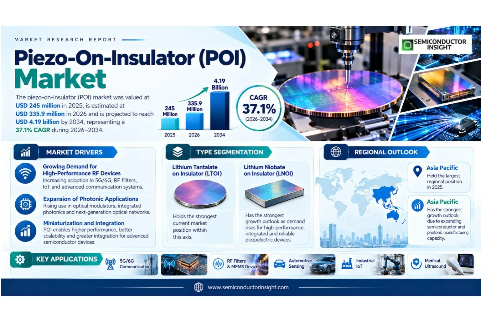
- The piezo-on-insulator POI market was valued at USD 245 million in 2025, is estimated at USD 335.9 million in 2026 and is projected to reach USD 4.19 billion by 2034, representing a 37.1% CAGR during 2026–2034.
- Lithium Tantalate on Insulator (LTOI) represents the leading type, while Lithium Niobate on Insulator (LNOI) offers the strongest growth momentum because buyer requirements are shifting toward higher integration, flexibility and performance within the product architecture.
- SAW Filters provides the largest application base, while Electro-Optic Modulators is developing faster as users prioritize measurable operating outcomes and application-specific functionality rather than generic hardware capability.
- Asia Pacific is the largest regional market in 2025, supported by largest downstream RF-filter and electronics manufacturing ecosystem, with strong POI adoption and expanding specialty-substrate supply. Asia Pacific has the fastest growth outlook as investment, adoption and supply ecosystems broaden.
- The principal growth mechanism is 5G and Wi-Fi filter complexity. It changes the economic case for adoption by improving utilization, performance or lifecycle value rather than relying on replacement demand alone.
- A meaningful restraint is High process complexity. Suppliers that reduce this barrier through integration support, qualification evidence and clearer total-cost economics are better placed to convert technical interest into repeatable commercial deployments.
Piezo-On-Insulator (POI) Market Overview
Piezo-on-insulator POI market was valued at USD 245 million in 2025, is estimated at USD 335.9 million in 2026 and is projected to reach USD 4.19 billion by 2034, representing a 37.1% CAGR during 2026–2034. Asia Pacific held the largest regional position in 2025, while Asia Pacific has the strongest growth outlook.
Base year: 2025 · Estimated year: 2026 · Forecast period: 2026–2034 · Values in USD million unless stated otherwise
Piezo-on-insulator is an engineered substrate in which a thin single-crystal piezoelectric layer, commonly lithium tantalate or lithium niobate, is bonded above an insulating layer and a mechanically robust handle wafer. The architecture confines acoustic energy, improves temperature behavior and enables high-performance surface-acoustic-wave filters. Commercial value depends on crystalline quality, layer uniformity, wafer diameter, defect control and compatibility with high-volume lithography, packaging and RF front-end assembly.
POI is moving from specialist material into a volume RF platform. Soitec reported that POI became its fourth product to generate annual revenue of around $100 million or more in fiscal 2025, with ten customers in volume production and thirteen in qualification. The company also lists its Bernin 3 fab at up to 0.7 million wafers per year of POI capacity. This combination of customer qualification and manufacturing scale materially reduces supply risk for filter makers considering broader adoption.
Segment Analysis: By Type
By Type segmentation comprises Lithium Niobate on Insulator (LNOI), Lithium Tantalate on Insulator (LTOI). Lithium Tantalate on Insulator (LTOI) holds the strongest current market position within this axis, while Lithium Niobate on Insulator (LNOI) has the strongest growth outlook. The distinction reflects differences in purchasing triggers, technical requirements and qualification intensity rather than a uniform shift across all customer groups. Type-level competition is therefore determined by architecture, performance and lifecycle economics at the product-design stage.
| Type | Market role | Commercial and technical analysis |
|---|---|---|
| Lithium Niobate on Insulator (LNOI) | Fastest-growing segment | Lithium Niobate on Insulator (LNOI) combines a thin piezoelectric layer with an insulating stack so device designers can engineer acoustic confinement, electromechanical coupling and feature dimensions beyond conventional bulk substrates. Selection depends on the targeted filter band, process integration and customer-qualified wafer specifications. The commercial barrier is not only crystal supply; it includes bonding quality, layer uniformity, wafer-scale defect control and repeatability across high-volume RF manufacturing. |
| Lithium Tantalate on Insulator (LTOI) | Leading segment | Lithium Tantalate on Insulator (LTOI) combines a thin piezoelectric layer with an insulating stack so device designers can engineer acoustic confinement, electromechanical coupling and feature dimensions beyond conventional bulk substrates. Selection depends on the targeted filter band, process integration and customer-qualified wafer specifications. The commercial barrier is not only crystal supply; it includes bonding quality, layer uniformity, wafer-scale defect control and repeatability across high-volume RF manufacturing. |
Segment Analysis: By Application
By Application segmentation comprises SAW Filters, Electro-Optic Modulators, Others. SAW Filters holds the strongest current market position within this axis, while Electro-Optic Modulators has the strongest growth outlook. The distinction reflects differences in purchasing triggers, technical requirements and qualification intensity rather than a uniform shift across all customer groups. Application-level demand follows the operating problem being solved, so adoption speed varies with the measurable value delivered to users.
| Application | Market role | Commercial and technical analysis |
|---|---|---|
| SAW Filters | Leading segment | SAW Filters represents a demand path where POI can improve device performance by exploiting thin-film piezoelectric behavior and engineered acoustic or optical confinement. Adoption occurs only after device makers redesign structures around the substrate and complete qualification, so revenue ramps lag technical demonstrations. Suppliers benefit when a platform is designed into high-volume components, but switching suppliers later can be difficult because wafer properties are tightly coupled to process recipes and device performance. |
| Electro-Optic Modulators | Fastest-growing segment | Electro-Optic Modulators represents a demand path where POI can improve device performance by exploiting thin-film piezoelectric behavior and engineered acoustic or optical confinement. Adoption occurs only after device makers redesign structures around the substrate and complete qualification, so revenue ramps lag technical demonstrations. Suppliers benefit when a platform is designed into high-volume components, but switching suppliers later can be difficult because wafer properties are tightly coupled to process recipes and device performance. |
| Others | Established segment | Others represents a demand path where POI can improve device performance by exploiting thin-film piezoelectric behavior and engineered acoustic or optical confinement. Adoption occurs only after device makers redesign structures around the substrate and complete qualification, so revenue ramps lag technical demonstrations. Suppliers benefit when a platform is designed into high-volume components, but switching suppliers later can be difficult because wafer properties are tightly coupled to process recipes and device performance. |
Additional Segment Analysis: By Wafer Size
By Wafer Size segmentation comprises 4-inch, 6-inch, Others. 6-inch holds the strongest current market position within this axis, while Other larger formats has the strongest growth outlook. The distinction reflects differences in purchasing triggers, technical requirements and qualification intensity rather than a uniform shift across all customer groups. Wafer diameter affects tool compatibility, die economics and the qualification path required to move specialty materials into higher-volume production.
| Wafer Size | Market role | Commercial and technical analysis |
|---|---|---|
| 4-inch | Established segment | 4-inch is an important wafer size category because it changes the purchasing criteria, qualification path and value captured by suppliers. Customers evaluate compatibility with the wider system, lifecycle support and operating performance rather than treating the category as interchangeable. Market growth in this segment therefore depends on design-in activity and application-specific proof points. Suppliers with documented performance and integration support are better positioned than vendors competing on unit price alone. |
| 6-inch | Leading segment | 6-inch is an important wafer size category because it changes the purchasing criteria, qualification path and value captured by suppliers. Customers evaluate compatibility with the wider system, lifecycle support and operating performance rather than treating the category as interchangeable. Market growth in this segment therefore depends on design-in activity and application-specific proof points. Suppliers with documented performance and integration support are better positioned than vendors competing on unit price alone. |
| Others | Established segment | Others is an important wafer size category because it changes the purchasing criteria, qualification path and value captured by suppliers. Customers evaluate compatibility with the wider system, lifecycle support and operating performance rather than treating the category as interchangeable. Market growth in this segment therefore depends on design-in activity and application-specific proof points. Suppliers with documented performance and integration support are better positioned than vendors competing on unit price alone. |
Additional Segment Analysis: By Piezo-Layer Thickness
By Piezo-Layer Thickness segmentation comprises 100nm-900nm, 1μm-20μm, Others. 100nm-900nm holds the strongest current market position within this axis, while 1μm-20μm has the strongest growth outlook. The distinction reflects differences in purchasing triggers, technical requirements and qualification intensity rather than a uniform shift across all customer groups. Layer thickness directly shapes device design freedom and process control, so suppliers must hold tight uniformity across qualified wafer lots.
| Piezo-Layer Thickness | Market role | Commercial and technical analysis |
|---|---|---|
| 100nm-900nm | Leading segment | 100nm-900nm is an important piezo-layer thickness category because it changes the purchasing criteria, qualification path and value captured by suppliers. Customers evaluate compatibility with the wider system, lifecycle support and operating performance rather than treating the category as interchangeable. Market growth in this segment therefore depends on design-in activity and application-specific proof points. Suppliers with documented performance and integration support are better positioned than vendors competing on unit price alone. |
| 1μm-20μm | Fastest-growing segment | 1μm-20μm is an important piezo-layer thickness category because it changes the purchasing criteria, qualification path and value captured by suppliers. Customers evaluate compatibility with the wider system, lifecycle support and operating performance rather than treating the category as interchangeable. Market growth in this segment therefore depends on design-in activity and application-specific proof points. Suppliers with documented performance and integration support are better positioned than vendors competing on unit price alone. |
| Others | Established segment | Others is an important piezo-layer thickness category because it changes the purchasing criteria, qualification path and value captured by suppliers. Customers evaluate compatibility with the wider system, lifecycle support and operating performance rather than treating the category as interchangeable. Market growth in this segment therefore depends on design-in activity and application-specific proof points. Suppliers with documented performance and integration support are better positioned than vendors competing on unit price alone. |
Regional Analysis
Asia Pacific leads the market in 2025, while Asia Pacific has the fastest growth outlook. Regional demand differs materially because end-market investment, local manufacturing, qualification practices, channel structure and customer economics are not uniform. The comparison below treats each geography according to its own commercial mechanism rather than repeating one global narrative with different country names.
How does regional demand differ across the Piezo-On-Insulator (POI) market?
Regional strategy depends on where design decisions are made, where end users deploy equipment, and how local customers evaluate lifecycle value. Asia Pacific benefits from largest downstream RF-filter and electronics manufacturing ecosystem, with strong POI adoption and expanding specialty-substrate supply. Asia Pacific is expanding more quickly because new adoption, local supply capabilities and application investment are broadening from a smaller or less mature base. Other regions remain relevant where regulation, installed base or specialized end markets create defensible demand.
| Region | Position | Growth outlook | Demand profile | Primary market logic |
|---|---|---|---|---|
| Asia Pacific | Largest & fastest | Highest | RF-filter manufacturing led | Asia Pacific leads because smartphone, RF front-end, electronics and specialty-material supply chains are concentrated in the region. |
| Europe | Strategic supply hub | High | Specialty-substrate led | Europe’s role is shaped by advanced materials rather than sheer downstream device volume. |
| North America | Innovation market | High | Design and photonics led | North America is important for RF design, integrated photonics, device startups and wireless system architecture. |
| South America | Small | Moderate | Imported electronics led | Direct POI wafer consumption is limited because the region has a smaller advanced RF-filter and specialty-substrate manufacturing base. |
| Middle East & Africa | Early stage | Moderate | Telecom and research led | The region is a small direct substrate market but has selective opportunities in telecom, satellite systems, research and semiconductor-design initiatives. |
Detailed Regional Blocks
Competitive Landscape
The competitive barrier is not simply access to lithium tantalate or lithium niobate; it is repeatable layer transfer, wafer-scale uniformity, low defect density and the ability to qualify with RF-filter customers. Soitec differentiates through Smart Cut technology and established volume capacity, while Chinese suppliers are building domestic thin-film capability. Traditional silicon-wafer companies are adjacent participants, but leadership in POI requires piezoelectric materials expertise and process integration that is different from commodity silicon substrate manufacturing.
Competition in the piezo-on-insulator (poi) market is shaped by design-in relationships, system integration and the cost of switching after qualification. Buyers do not evaluate suppliers solely on headline specifications. They also examine reliability, documentation, software or process compatibility, support response and the ability to maintain performance over the full product lifecycle. This favors vendors that can combine technical differentiation with repeatable delivery and customer engineering support.
The market includes established specialists, vertically integrated technology suppliers and emerging firms pursuing narrower application niches. The competitive boundary is therefore fluid: a supplier can lead in one segment without controlling the whole market. Partnerships, standards participation and ecosystem integration often matter as much as manufacturing scale because customers need assurance that a selected solution will remain compatible with future platforms and deployment requirements.
| Competitive group | Representative companies | Strategic position |
|---|---|---|
| Established / scale suppliers | Soitec, Jinan Jingzheng Electronics (NANOLN), Shanghai Novel Si Integration Technology, Beijing Qinghe Jingyuan | Compete on broad customer access, installed base, qualification history and global support. |
| Technology-focused challengers | NGK Insulators, IOPTEE, PAM-Xiamen, Partow Technologies | Compete through technical differentiation, product focus and faster adaptation to emerging requirements. |
| Specialists and ecosystem participants | GlobalWafers, Siltronic, Shin-Etsu Chemical, SUMCO, Okmetic | Serve specialized applications, regional demand or ecosystem roles that can be strategically important despite smaller scale. |
Profiled market participants
The profiled competitive set includes Soitec, Jinan Jingzheng Electronics (NANOLN), Shanghai Novel Si Integration Technology, Beijing Qinghe Jingyuan, NGK Insulators, IOPTEE, PAM-Xiamen, Partow Technologies, GlobalWafers, Siltronic, Shin-Etsu Chemical, SUMCO, Okmetic. The list spans suppliers with different scale, geographic exposure and product depth. Inclusion identifies commercial relevance to the market scope; it does not imply identical product coverage or an equal competitive position across every segment.
Production Capacity Analysis
POI capacity is more concentrated than conventional silicon wafers because the product requires specialized layer-transfer and bonding know-how. Soitec identifies Bernin 3 in France as a POI site with capacity up to 0.7 million wafers per year. The capacity challenge is therefore both quantitative and qualitative: additional wafer starts are useful only if thickness uniformity, crystal quality and RF performance remain within customer specifications. Yield learning and customer qualification can constrain effective supply even before physical tool capacity is fully utilized.
Capacity should be interpreted as the ability to deliver qualified, repeatable product rather than as nominal factory floor alone. In piezo-on-insulator (poi), bottlenecks can sit in specialized materials, precision manufacturing, software validation, bonding or packaging, calibration, test, or customer qualification depending on the segment. A supplier with unused physical capacity may still be constrained if the required process window, certifications or engineering support are not available for a customer’s exact design.
Market Dynamics
Growth is driven by the need for RF filters that combine wide bandwidth, low insertion loss, high quality factor and improved thermal behavior as wireless front ends become more complex. POI competes with bulk piezoelectric substrates, temperature-compensated SAW and BAW approaches, so adoption depends on frequency band, power handling, cost and integration architecture. The market expands fastest when POI allows filter designers to consolidate functions or meet performance that is difficult to achieve with established substrates.
Market Drivers
| Driver | Relative influence | Why it matters |
|---|---|---|
| 5G and Wi-Fi filter complexity | High | Mobile and connected devices must isolate an increasing number of closely spaced radio bands while preserving battery life and signal quality. Soitec positions POI for low-band and mid-high-band filters, including 150 mm and 200 mm products. Better acoustic confinement and thermal behavior can reduce insertion loss and improve selectivity. The commercial driver is therefore not simply more smartphones; it is rising RF complexity per device and the value of high-performance front-end filtering. |
| Transition to multilayer SAW | High | SAW on POI allows filter designers to engineer the substrate stack rather than rely only on bulk piezoelectric material properties. This can improve quality factor, coupling and temperature coefficient while retaining manufacturing techniques familiar to the SAW ecosystem. The transition supports higher-value engineered wafers because substrate performance directly affects filter specifications. As customers qualify multilayer SAW platforms, demand can scale quickly across multiple bands and device generations. |
| Larger wafer formats | Medium to High | Moving from 100 mm toward 150 mm and 200 mm formats increases die output per wafer and improves compatibility with higher-throughput manufacturing. Soitec lists both 150 mm and 200 mm POI products, showing that industrialization is progressing beyond small research wafers. Larger formats require tighter global uniformity and equipment compatibility, but once qualified they improve economics and can accelerate adoption among high-volume filter manufacturers. |
| Customer qualification momentum | Medium | Specialty substrates face long qualification cycles because changes can affect RF performance, assembly yield and long-term reliability. Soitec’s fiscal 2025 disclosure of ten customers in volume production and thirteen in qualification indicates a widening commercial pipeline. Each successful qualification can create multi-year demand because RF filter platforms are tied to device roadmaps. This makes design wins and process stability more important than spot wafer pricing. |
5G and Wi-Fi filter complexity
Mobile and connected devices must isolate an increasing number of closely spaced radio bands while preserving battery life and signal quality. Soitec positions POI for low-band and mid-high-band filters, including 150 mm and 200 mm products. Better acoustic confinement and thermal behavior can reduce insertion loss and improve selectivity. The commercial driver is therefore not simply more smartphones; it is rising RF complexity per device and the value of high-performance front-end filtering.
Transition to multilayer SAW
SAW on POI allows filter designers to engineer the substrate stack rather than rely only on bulk piezoelectric material properties. This can improve quality factor, coupling and temperature coefficient while retaining manufacturing techniques familiar to the SAW ecosystem. The transition supports higher-value engineered wafers because substrate performance directly affects filter specifications. As customers qualify multilayer SAW platforms, demand can scale quickly across multiple bands and device generations.
Larger wafer formats
Moving from 100 mm toward 150 mm and 200 mm formats increases die output per wafer and improves compatibility with higher-throughput manufacturing. Soitec lists both 150 mm and 200 mm POI products, showing that industrialization is progressing beyond small research wafers. Larger formats require tighter global uniformity and equipment compatibility, but once qualified they improve economics and can accelerate adoption among high-volume filter manufacturers.
Customer qualification momentum
Specialty substrates face long qualification cycles because changes can affect RF performance, assembly yield and long-term reliability. Soitec’s fiscal 2025 disclosure of ten customers in volume production and thirteen in qualification indicates a widening commercial pipeline. Each successful qualification can create multi-year demand because RF filter platforms are tied to device roadmaps. This makes design wins and process stability more important than spot wafer pricing.
Market Restraints
| Restraint | Relative influence | Commercial effect |
|---|---|---|
| High process complexity | High | Producing a thin, uniform single-crystal piezoelectric layer on an insulating stack requires advanced bonding, thinning or layer-transfer processes and precise metrology. Small thickness or defect variations can alter acoustic performance across a wafer. This creates high capital intensity, process-development cost and yield sensitivity. New entrants therefore need more than raw material access; they need a reproducible manufacturing platform and customer confidence in lot-to-lot consistency. |
| Long RF qualification cycles | Medium to High | Filter makers must validate material uniformity, resonator performance, packaging compatibility and reliability before committing a substrate to volume production. Qualification can span multiple product generations and may require close co-development. This slows supplier switching and raises the cost of entering an incumbent account. It also means announced capacity does not immediately translate into revenue because the qualified customer base can be the binding constraint. |
| Competing acoustic technologies | Medium | BAW, TC-SAW and advanced bulk-substrate designs continue to improve and already serve major RF bands. POI must deliver a meaningful performance or integration advantage at a competitive total device cost. Not every band or power requirement favors the same acoustic technology. The result is a segmented market in which POI expands strongly in suitable frequency ranges but coexists with other filter platforms rather than replacing them universally. |
| Specialty-material supply concentration | Medium | High-quality lithium tantalate and lithium niobate crystal supply, bonding expertise and specialized processing are concentrated among a limited set of companies and regions. Rapid demand growth can therefore create qualification or lead-time pressure even if end-market demand is strong. Customers may pursue second sources, but duplicating acoustic performance across different substrate stacks is technically demanding. Supply assurance becomes a strategic purchasing factor. |
High process complexity
Producing a thin, uniform single-crystal piezoelectric layer on an insulating stack requires advanced bonding, thinning or layer-transfer processes and precise metrology. Small thickness or defect variations can alter acoustic performance across a wafer. This creates high capital intensity, process-development cost and yield sensitivity. New entrants therefore need more than raw material access; they need a reproducible manufacturing platform and customer confidence in lot-to-lot consistency.
Long RF qualification cycles
Filter makers must validate material uniformity, resonator performance, packaging compatibility and reliability before committing a substrate to volume production. Qualification can span multiple product generations and may require close co-development. This slows supplier switching and raises the cost of entering an incumbent account. It also means announced capacity does not immediately translate into revenue because the qualified customer base can be the binding constraint.
Competing acoustic technologies
BAW, TC-SAW and advanced bulk-substrate designs continue to improve and already serve major RF bands. POI must deliver a meaningful performance or integration advantage at a competitive total device cost. Not every band or power requirement favors the same acoustic technology. The result is a segmented market in which POI expands strongly in suitable frequency ranges but coexists with other filter platforms rather than replacing them universally.
Specialty-material supply concentration
High-quality lithium tantalate and lithium niobate crystal supply, bonding expertise and specialized processing are concentrated among a limited set of companies and regions. Rapid demand growth can therefore create qualification or lead-time pressure even if end-market demand is strong. Customers may pursue second sources, but duplicating acoustic performance across different substrate stacks is technically demanding. Supply assurance becomes a strategic purchasing factor.
Market Opportunities
200 mm POI
The move toward 200 mm substrates can materially improve manufacturing throughput and align POI with more automated semiconductor production. Soitec already lists 200 mm lithium-tantalate POI products for low- and mid-high-band RF filters. Wider adoption would expand wafer value and favor suppliers with mature large-diameter bonding and uniformity control. It also creates equipment opportunities in metrology, handling and process control tailored to piezoelectric multilayers.
Electro-optic photonics
Lithium-niobate-based thin films are attractive for electro-optic modulators because of strong electro-optic properties and the potential for compact integrated photonic devices. This application diversifies POI beyond smartphone RF filters and exposes suppliers to data-center interconnect, sensing and emerging photonic systems. The market requirements differ from acoustic filters, so suppliers can build separate value propositions around optical loss, film orientation and photonic fabrication compatibility.
Non-terrestrial and satellite connectivity
Satellite and non-terrestrial networks increase pressure on RF front ends to handle additional bands, strong interference environments and power constraints. Soitec explicitly positions POI for mobile, IoT, non-terrestrial-network and satellite communications. Compact, selective filters with good thermal performance can gain value as devices support more simultaneous radio standards. This expands demand beyond conventional smartphone replacement cycles.
Sensor and ultrasonic devices
Thin piezoelectric films can support ultrasonic transducers, resonant sensors and energy-conversion devices that benefit from strong coupling and semiconductor-compatible substrates. These applications are smaller than RF filters today but can create higher-value niches and reduce dependence on mobile demand. The opportunity is strongest where device designers need integration, miniaturization and precise film thickness rather than low-cost bulk piezoelectric material.
Supply Chain Analysis
Upstream inputs
Core manufacturing
System integration & channels
End use & lifecycle
Upstream inputs
Materials, components, intellectual property and enabling production inputs define the technical ceiling and cost structure. Supplier concentration at this stage can affect lead times and qualification risk even when final assembly is geographically diversified. In the piezo-on-insulator (poi) market, the balance of value shifts toward suppliers that solve integration and qualification problems instead of merely supplying an interchangeable physical component.
Core manufacturing
Fabrication, assembly, bonding, calibration, software integration or precision manufacturing converts inputs into a qualified product. Yield, process control and test discipline determine whether nominal capacity becomes saleable output. In the piezo-on-insulator (poi) market, the balance of value shifts toward suppliers that solve integration and qualification problems instead of merely supplying an interchangeable physical component.
System integration & channels
OEMs, equipment builders, distributors, software platforms and integrators connect the product with the customer’s operating environment. This stage captures value through application engineering, configuration, distribution reach and support. In the piezo-on-insulator (poi) market, the balance of value shifts toward suppliers that solve integration and qualification problems instead of merely supplying an interchangeable physical component.
End use & lifecycle
End users monetize the technology through productivity, performance, reliability or user outcomes. Replacement, subscriptions, maintenance, upgrades and installed-base support determine how much recurring value remains after the initial sale. In the piezo-on-insulator (poi) market, the balance of value shifts toward suppliers that solve integration and qualification problems instead of merely supplying an interchangeable physical component.
Recent Developments
Soitec reported that POI became its fourth product to generate annual revenue of around $100 million or more. The company also stated that ten customers were in volume production and thirteen additional customers were in qualification. This is a major commercialization signal because specialty substrates move from pilot status to a repeatable market only when multiple customers complete qualification and volume ramps.
Soitec’s manufacturing information lists Bernin 3 in France as its POI facility with capacity up to 0.7 million wafers per year. The disclosed scale provides a visible industrial supply base for customers adopting multilayer SAW technologies. It also raises the competitive bar for new entrants because customers can compare qualification risk against an established high-volume manufacturing platform.
Soitec’s Connect POI portfolio includes 150 mm lithium-tantalate and lithium-niobate products and 200 mm lithium-tantalate products for RF filters. The larger wafer roadmap indicates ongoing industrialization and supports lower unit processing cost as demand scales. It also broadens the addressable set of filter manufacturers whose equipment and automation are optimized for larger diameters.
Report Scope & Segmentation
This market overview covers the commercial value of piezo-on-insulator (poi) across the defined product, application and buyer segmentation. The scope uses 2025 as the base year, 2026 as the estimated year and 2026–2034 as the forecast period. It distinguishes market revenue from adjacent system value and uses qualitative leadership language where public evidence does not support a reliable numerical share.
| Scope attribute | Coverage |
|---|---|
| Base year | 2025 |
| Estimated year | 2026 |
| Forecast period | 2026–2034 |
| 2025 market size | USD 245 million |
| 2026 estimated size | USD 335.9 million |
| 2034 projected size | USD 4.19 billion |
| CAGR (2026–2034) | 37.1% |
| Largest market in 2025 | Asia Pacific |
| By Type | Lithium Niobate on Insulator (LNOI), Lithium Tantalate on Insulator (LTOI) |
| By Application | SAW Filters, Electro-Optic Modulators, Others |
| By Wafer Size | 4-inch, 6-inch, Others |
| By Piezo-Layer Thickness | 100nm-900nm, 1μm-20μm, Others |
| Regions | North America; Europe; Asia Pacific; South America; Middle East & Africa |
| Profiled companies | Soitec, Jinan Jingzheng Electronics (NANOLN), Shanghai Novel Si Integration Technology, Beijing Qinghe Jingyuan, NGK Insulators, IOPTEE, PAM-Xiamen, Partow Technologies, GlobalWafers, Siltronic, Shin-Etsu Chemical, SUMCO, Okmetic |
Frequently Asked Questions
What is the size of the Piezo-On-Insulator (POI) market?
The global piezo-on-insulator (poi) market was valued at USD 245 million in 2025, is estimated at USD 335.9 million in 2026 and is projected to reach USD 4.19 billion by 2034. This represents a 37.1% CAGR during 2026–2034. The forecast reflects increasing adoption within the defined product and application scope rather than the value of broader adjacent systems.
Which region leads the Piezo-On-Insulator (POI) market?
Asia Pacific holds the largest market position in 2025, supported by largest downstream RF-filter and electronics manufacturing ecosystem, with strong POI adoption and expanding specialty-substrate supply. The region combines demand, supplier access and customer readiness in a way that gives it a stronger current revenue base than other geographies. Regional leadership should be interpreted through those structural factors rather than as an unsupported universal percentage.
Which region is growing fastest?
Asia Pacific has the fastest growth outlook within the forecast period. The region benefits from expanding technology adoption, new investment, local supply development and broader application deployment. Growth does not imply that every country follows the same trajectory; qualification practices, purchasing power, infrastructure and end-market concentration continue to create substantial differences inside the region.
Which product type currently has the strongest position?
Lithium Tantalate on Insulator (LTOI) has the strongest current position within the By Type segmentation. Its leadership reflects established customer use, application fit and a larger installed or design-in base. Lithium Niobate on Insulator (LNOI) has the stronger growth outlook as product architectures evolve. Supplier success depends on matching performance and lifecycle support to the specific requirements of each type.
Which application is most important?
SAW Filters is the largest application segment within the defined scope because it provides the broadest current demand base. Electro-Optic Modulators has the stronger growth outlook as customers place greater value on specialized outcomes and deeper integration. The application mix matters commercially because purchasing triggers, qualification requirements and willingness to pay differ significantly between use cases.
What is the primary market driver?
5G and Wi-Fi filter complexity is a principal growth driver. Mobile and connected devices must isolate an increasing number of closely spaced radio bands while preserving battery life and signal quality. Soitec positions POI for low-band and mid-high-band filters, including 150 mm and 200 mm products. Better acoustic confinement and thermal behavior can reduce insertion loss and improve selectivity. The commercial driver is therefore not simply more smartphones; it is rising RF complexity per device and the value of high-performance front-end filtering. The effect is commercially meaningful because adoption accelerates when the technology improves measurable performance or lifecycle economics rather than simply adding a new feature.
What is the main restraint on market growth?
High process complexity is a significant restraint. Producing a thin, uniform single-crystal piezoelectric layer on an insulating stack requires advanced bonding, thinning or layer-transfer processes and precise metrology. Small thickness or defect variations can alter acoustic performance across a wafer. This creates high capital intensity, process-development cost and yield sensitivity. New entrants therefore need more than raw material access; they need a reproducible manufacturing platform and customer confidence in lot-to-lot consistency. Suppliers can reduce the barrier through clearer value proof, integration support, qualification evidence and product architectures that lower total lifecycle risk for customers.
How is competition structured?
The competitive barrier is not simply access to lithium tantalate or lithium niobate; it is repeatable layer transfer, wafer-scale uniformity, low defect density and the ability to qualify with RF-filter customers. Soitec differentiates through Smart Cut technology and established volume capacity, while Chinese suppliers are building domestic thin-film capability. Traditional silicon-wafer companies are adjacent participants, but leadership in POI requires piezoelectric materials expertise and process integration that is different from commodity silicon substrate manufacturing. Buyers also consider integration support, qualification history, reliability and ecosystem compatibility, which means market share is not determined by a single technical specification. Competition therefore varies by application and customer class, with established suppliers and focused specialists often holding different advantages.
Why is supply capacity strategically important?
POI capacity is more concentrated than conventional silicon wafers because the product requires specialized layer-transfer and bonding know-how. Soitec identifies Bernin 3 in France as a POI site with capacity up to 0.7 million wafers per year. The capacity challenge is therefore both quantitative and qualitative: additional wafer starts are useful only if thickness uniformity, crystal quality and RF performance remain within customer specifications. Yield learning and customer qualification can constrain effective supply even before physical tool capacity is fully utilized. Capacity matters because qualified output, not nominal floor space, determines what customers can actually buy. Yield, testing, specialized materials, software or process integration and customer approvals can all constrain shipment growth even when a supplier has physical expansion room.
What should buyers and suppliers watch through 2034?
Stakeholders should watch the pace of qualification, integration into wider ecosystems, regional investment, standards or certification changes, and the ability of suppliers to convert technical capability into repeatable production and lifecycle support. The strongest opportunities will emerge where performance gains are measurable and customer switching costs support durable relationships without creating unacceptable adoption friction.
Research Sources & Evidence Base
View research sources used for this overview.
- Soitec. Connect POI Substrates — Product architecture, wafer sizes, RF-filter positioning and manufacturing compatibility.
- Soitec. Fiscal Year 2025 Results — POI revenue milestone, customer volume production and qualification.
- Soitec. Semiconductor Fabs — Bernin 3 POI manufacturing capacity.
- Soitec. Mobile Communications — POI position in mobile 5G and Wi-Fi applications.
Get Sample Report PDF for Exclusive Insights
Report Sample Includes
- Table of Contents
- List of Tables & Figures
- Charts, Research Methodology, and more...




