Photomask Inspection Equipment Market Insights
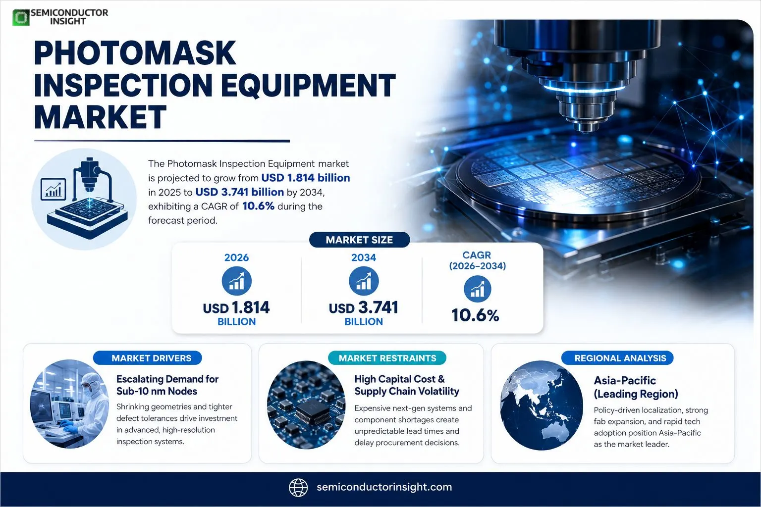
Photomask Inspection Equipment market size was valued at USD 1.814 billion in 2025. The market is forecasted to reach USD 3.741 billion by 2034, showing a CAGR of 10.6 % over the forecast horizon.
Photomask inspection equipment comprise high‑precision optical and e‑beam systems that examine photomasks for pattern defects exceeding lithography tolerances. These tools enable detection of pinholes, line‑edge roughness and overlay errors, ensuring that masks used as masters for integrated‑circuit fabrication meet stringent specifications.Growth is fueled by rising demand for sub‑7 nm AI compute chips and ultra‑high‑resolution display masks, which push requirements for finer defect detection. Advances in high‑NA EUV lithography and the emergence of curved mask designs create new technical challenges that spur equipment upgrades. Meanwhile, Asia‑Pacific manufacturers accelerate localization effortsespecially in Chinaexpanding domestic supply chains. Integration of artificial intelligence algorithms for defect classification and increased automation further enhance inspection throughput and accuracy.
MARKET DRIVERS
Escalating Demand for Sub‑10 nm Nodes
Photomask Inspection Equipment Market is feeling the pressure of semiconductor fabs pushing toward sub‑10 nm technology. As pattern dimensions shrink, defect tolerances tighten, prompting manufacturers to invest in higher‑resolution inspection tools that can detect sub‑20 nm anomalies. This shift not only spurs equipment upgrades but also expands service contracts for calibration and maintenance.
Stringent Yield Targets in Advanced Logic
Yield optimization has become a board‑level KPI, especially for high‑margin logic chips. A modest 0.5 % defect density improvement can translate into millions of dollars in profit, encouraging fabs to prioritize comprehensive mask verification. Consequently, vendors are introducing AI‑assisted analytics that reduce false‑positive rates and shorten cycle times.
➤ “Clients that adopted inline inspection saw a 12 % reduction in mask‑related rework within the first six months.”
Regulatory scrutiny over product reliability, especially in automotive and medical silicon, adds another layer of urgency. Compliance audits now request documented mask integrity, nudging end‑users toward higher‑specification inspection platforms and creating a virtuous loop of equipment demand.
MARKET CHALLENGES
Capital Intensity of Next‑Gen Systems
Acquiring state‑of‑the‑art inspection units often requires multi‑million‑dollar outlays, a hurdle for midsize fabs operating on thin margins. The steep amortization schedules can deter early adoption, slowing the overall market tempo despite clear technical benefits.
Other Challenges
Skill Shortage
Operating sophisticated optics and interpreting high‑resolution data demand specialized expertise. Many organizations find themselves scrambling to train engineers, which can elongate implementation timelines and increase reliance on external consultants.
Furthermore, the rapid cadence of technology nodes forces equipment makers to compress development cycles, sometimes leading to trade‑offs between performance and reliability in the first generation of a product line.
MARKET RESTRAINTS
Supply‑Chain Volatility
Component shortagesparticularly for high‑precision lenses and specialized detectorshave introduced unpredictable lead times. When a critical part is delayed, entire installation projects stall, eroding confidence among prospective buyers and prompting them to defer purchases.
Regulatory Compliance Costs
Emerging environmental regulations around hazardous materials used in some inspection systems are raising compliance expenditures. Companies must invest in waste‑management protocols and certification processes, adding incremental overhead that can suppress net‑new spending.
MARKET OPPORTUNITIES
Integration of Machine‑Learning Analytics
Embedding machine‑learning models into inspection workflows presents a fertile growth niche. Predictive defect classification can cut review times by up to 30 %, a compelling value proposition for fabs eager to speed time‑to‑market. Vendors that package these analytics as a service stand to capture recurring revenue streams.
Expansion into Emerging Foundries
Newfoundry entrants in Southeast Asia and Eastern Europe are constructing modern fabs with a bias toward advanced nodes. Their equipment procurement plans frequently allocate a sizable share to mask inspection, offering a fresh customer base for established players willing to tailor financing structures.Lastly, the rise of photonic integrated circuits introduces distinct mask‑verification requirements, including novel materials and pattern geometries. Early movers that adapt inspection optics to these demands could secure a first‑mover advantage and diversify revenue beyond traditional semiconductor applications.
Photomask Inspection Equipment Market Trends
Demand‑Driven: AI Chip Boom and High‑Resolution Displays
The surge in AI compute chips and ultra‑high‑definition display panels has forced mask manufacturers to tighten tolerances beyond traditional limits. When a chip design moves below the 7 nm node, even a nanometer‑scale defect can corrupt yield, prompting fabs to seek inspection tools that resolve sub‑nanometer features. Simultaneously, 4K/8K panel makers require mask patterns that sustain large‑area uniformity, driving orders for equipment that can scan larger fields without sacrificing precision. In 2025, production of Photomask Inspection Equipment reached 310 units, each priced around US$6.4 million, underscoring how customers are willing to invest heavily in capability that directly protects wafer output. This buying behavior reinforces Photomask Inspection Equipment Market’s shift toward premium, high‑resolution solutions.
Other Trends
Technological Iteration: EUV and Curved Masks
High‑NA extreme ultraviolet (EUV) lithography is reshaping the inspection landscape. As manufacturers migrate from 13.5 nm to 13 nm and beyond, mask defects become harder to detect with conventional optics, prompting vendors to embed higher numerical‑aperture lenses and advanced alignment algorithms. At the same time, a niche of curved mask production has emerged to mitigate focus variation in next‑generation steppers. Curved substrates demand inspection heads that can accommodate non‑planar geometry while preserving angular accuracy, a capability only a few suppliers have demonstrated. The convergence of these two technologies is compelling equipment makers to redesign mechanical stages and software stacks, a move that will likely differentiate leaders within Photomask Inspection Equipment Market over the next decade.
Regional Growth and Intelligent Upgrade
Asia‑Pacific, led by China, is consolidating its role as the world’s largest consumer of inspection tools. Policy initiatives aimed at reducing reliance on imported semiconductor components have spurred domestic investment in mask‑related infrastructure, and local manufacturers are rapidly expanding their product portfolios. Parallel to this geographic thrust, the industry is embedding artificial intelligence and full‑process automation into inspection workflows. Machine‑learning models now assist in defect classification, reducing false‑positive rates and shortening cycle times, while robotic handling systems enable unattended operation from pre‑exposure through post‑inspection. These twin forcesregional localization and intelligent upgradeare redefining value chains and creating new entry points for vendors that can marry sophisticated AI algorithms with robust hardware, thereby shaping the future competitive dynamics of Photomask Inspection Equipment Market.
COMPETITIVE LANDSCAPEKey Industry Players
Photomask Inspection Equipment: Competitive Overview 2025‑2034
Among the tier‑one manufacturers, KLA Corp. dominates the high‑resolution segment, leveraging its AI‑driven defect classification engines and a service network that aligns with the surge in sub‑7nm mask requirements. Applied Materials follows closely, differentiating its portfolio through the integration of advanced illumination optics that accommodate both high‑NA EUV and emerging curved‑mask formats. Both firms benefit from deep install bases in semiconductor fabs, allowing them to capture incremental spend on equipment upgrades as design rules tighten. The market structure therefore reflects a duopolistic core, where scale, software sophistication, and localized support dictate bargaining power with OEM customers.Beyond the dominant duopoly, a tier of niche innovators sustains competitive pressure. Lasertec (Japan) and NuFlare (Japan) specialize in compact, high‑throughput inspection tools tailored for mask blanks and low‑volume production lines, carving out a steady share in Asia‑Pacific factories. Carl Zeiss AG (Germany) and Nikon (Japan) exploit their optical heritage to deliver ultra‑precise metrology modules that are increasingly paired with AI analytics from third‑party providers. Advantest, Visionoptech (China), Tokyo Electron, and Hitachi High‑Technologies each address specific regional demandsChina’s localization drive, South Korea’s high‑volume fabs, and Europe’s niche high‑accuracy applications. These players collectively broaden the supplier pool, forcing the leaders to continuously refine pricing, service contracts, and roadmap transparency.
List of Key Photomask Inspection Equipment Companies Profiled
- KLA Corp.
- Applied Materials
- Lasertec
- NuFlare
- Carl Zeiss AG
- Advantest
- Visionoptech
- Tokyo Electron
- Hitachi High‑Technologies
- Nikon
- R&P Instruments
- ASML (Metrology division)
- Synopsys (Defect analysis software)
- Nanometrics
- Fujifilm
Segment Analysis:
| Segment Category | Sub-Segments | Key Insights |
| By Type |
|
Photomask Detection Equipment continues to dominate because it directly addresses the demand for ultra‑high resolution defect detection required by next‑generation AI chips and high‑resolution displays.
|
| By Application |
|
Semiconductor Chip Manufacturer represents the most critical application area as chipmakers rely on flawless masks to sustain yield improvements.
|
| By End User |
|
Integrated Device Manufacturers lead the end‑user segment because they own both design and fabrication stages, mandating tight control over mask quality.
|
| By Technology |
|
High‑NA EUV Inspection is emerging as the technology frontier, driven by the push for finer patterning.
|
| By Market Trend |
|
AI and Automation Integration is reshaping the inspection workflow, delivering higher throughput and smarter defect handling.
|
Regional Analysis: Photomask Inspection Equipment Market
Asia‑Pacific
Taiwanese and Korean fabs have integrated next‑generation inspection modules within two years of release, shortening the typical technology cycle. This rapid adoption forces vendors to streamline firmware updates and provide modular upgrade paths, ensuring equipment remains compatible with evolving mask designs.
Universities in Singapore and Shanghai are producing graduates specialized in metrology and data analytics, feeding a talent pool that equipment makers tap for local support teams. The depth of expertise reduces downtime and enhances customer confidence in complex inspection workflows.
Recent geopolitical shifts have prompted manufacturers to source critical components from regional suppliers. This shift mitigates lead‑time volatility, allowing fabs to maintain consistent throughput despite broader market disruptions.
Local standards bodies are harmonising defect classification criteria, which simplifies cross‑border equipment certification and accelerates market entry for new inspection platforms across the Pacific basin.
North America
In the United States and Canada, Photomask Inspection Equipment Market is driven by a mature ecosystem of research institutions and a concentration of high‑volume logic fabs. Companies are emphasizing integration of machine‑learning algorithms to cope with shrinking pitch sizes, while also navigating stricter data‑security regulations that affect remote diagnostics. The presence of multiple tier‑1 equipment manufacturers creates a competitive pricing environment, compelling suppliers to differentiate through service quality and predictive maintenance contracts.
Europe
European fabs, particularly in Germany and the Netherlands, balance legacy 193‑nm lines with nascent EUV pilots. The region’s strong emphasis on sustainability translates into demand for inspection tools that minimise power consumption and waste. Collaborative ventures between equipment vendors and research consortia are fostering bespoke solutions for niche applications such as specialty memory, reinforcing Europe’s role as a hub for customized innovation.
South America
South American semiconductor activity remains modest, yet the region is witnessing incremental investments in advanced packaging that require precise mask verification. Local manufacturers are seeking cost‑effective inspection platforms that can be serviced remotely, leading to a rise in leasing models. The market’s trajectory will hinge on the ability of suppliers to offer scalable solutions that align with the region’s price sensitivity.
Middle East & Africa
The Middle East & Africa region is at an early stage of semiconductor fabrication, with several governments launching initiatives to build local fabs. Early adopters are focusing on defect‑reduction technologies that can accelerate yield ramp‑up. Partnerships between international equipment providers and regional technology parks are expected to create a foothold for advanced inspection capabilities, albeit with a strong emphasis on training and knowledge transfer.
Report Scope
This market research report provides a comprehensive analysis of the Photomask Inspection Equipment Market , covering the forecast period 2026–2034. It offers detailed insights into market dynamics, technological advancements, competitive landscape, and key trends shaping the industry.
Key focus areas of the report include:
- Market Overview: The report begins with an overview outlining its current market scenario, key growth indicators, and industry transformation drivers. It discusses macroeconomic factors, demand–supply balance, regulatory landscape, and the strategic role of semiconductors in powering advancements across industries such as automotive, telecommunications, consumer electronics, and industrial automation.
- Market Size & Forecast: Historical data and future projections for revenue, unit shipments, and market value across major regions and segments.
- Segmentation Analysis: Detailed breakdown by product type, technology, application, and end-user industry to identify high-growth segments and investment opportunities.
- Regional Insights: Insights into market performance across North America, Europe, Asia-Pacific, Latin America, and the Middle East & Africa, including country-level analysis where relevant.
- Competitive Landscape: Profiles of leading market participants, including their product offerings, R&D focus, manufacturing capacity, pricing strategies, and recent developments such as mergers, acquisitions, and partnerships.
- Technology Trends & Innovation: Assessment of emerging technologies, integration of AI/IoT, semiconductor design trends, fabrication techniques, and evolving industry standards.
- Market Drivers & Restraints: Evaluation of factors driving market growth along with challenges, supply chain constraints, regulatory issues, and market-entry barriers.
- Stakeholder Insights: Insights for component suppliers, OEMs, system integrators, investors, and policymakers regarding the evolving ecosystem and strategic opportunities.
Primary and secondary research methods are employed, including interviews with industry experts, data from verified sources, and real-time market intelligence to ensure the accuracy and reliability of the insights presented.
FREQUENTLY ASKED QUESTIONS:
What is the current market size of Photomask Inspection Equipment Market?
-> Photomask Inspection Equipment Market was valued at USD 1,814 million in 2025 and is expected to reach USD 3,741 million by 2034.
Which key companies operate in Photomask Inspection Equipment Market?
-> Key players include KLA (US), Applied Materials (US), Lasertec (JP), NuFlare (JP), Carl Zeiss AG (DE), Advantest (JP), Visionoptech (CN), among others.
What are the key growth drivers?
-> Key growth drivers include the surge in demand for high‑resolution masks driven by AI compute chips and 4K/8K display markets, technological iteration toward high‑NA EUV and curved masks, and accelerated localization in the Asia‑Pacific region.
Which region dominates the market?
-> Asia‑Pacific holds the largest share and is the fastest‑growing region, supported by strong policy‑driven localization, especially in China.
What are the emerging trends?
-> Emerging trends include integration of AI for defect discrimination and data mining, full‑process automation, and development of inspection equipment for high‑NA EUV and curved mask technologies.

Get Sample Report PDF for Exclusive Insights
Report Sample Includes
- Table of Contents
- List of Tables & Figures
- Charts, Research Methodology, and more...