Key Statistics
Key Takeaways
- Market trajectory: The RF-grade silicon carbide substrate market is valued at USD 212 million in 2025, with an estimated USD 249 million in 2026 and a forecast of USD 911 million by 2034, equivalent to a 17.6% compound annual growth rate from 2025 through 2034; purchases are concentrated in the demanding material platform for GaN microwave amplifiers.
- 6 Inch diameter: The 150 mm wafer class accounts for an estimated ~57% of the 2025 substrate revenue mix and is expected to advance at ~18.1% annually, reflecting the manufacturing compromise between available crystal quality and the number of RF amplifier dies obtained from each wafer.
- 8 Inch progression: The 200 mm category holds a modeled ~9% share but could expand at ~28.1% as device producers qualify larger epitaxial surfaces; technical availability must not be confused with routine high-volume shipments into RF fabrication.
- 5G Base Station: Telecommunications power amplifiers are the leading application with an estimated ~69% share, while LiDAR contributes ~12% and specialized microwave uses account for the remaining ~19% of the modeled revenue pool.
- Regional leadership: Asia-Pacific represents an estimated ~46% of market value and the highest modeled growth rate of ~19.0%; North America follows at ~26%, supported by high-value crystal production and RF-device engineering.
Silicon Carbide (SiC) Substrates for RF Device Market Overview
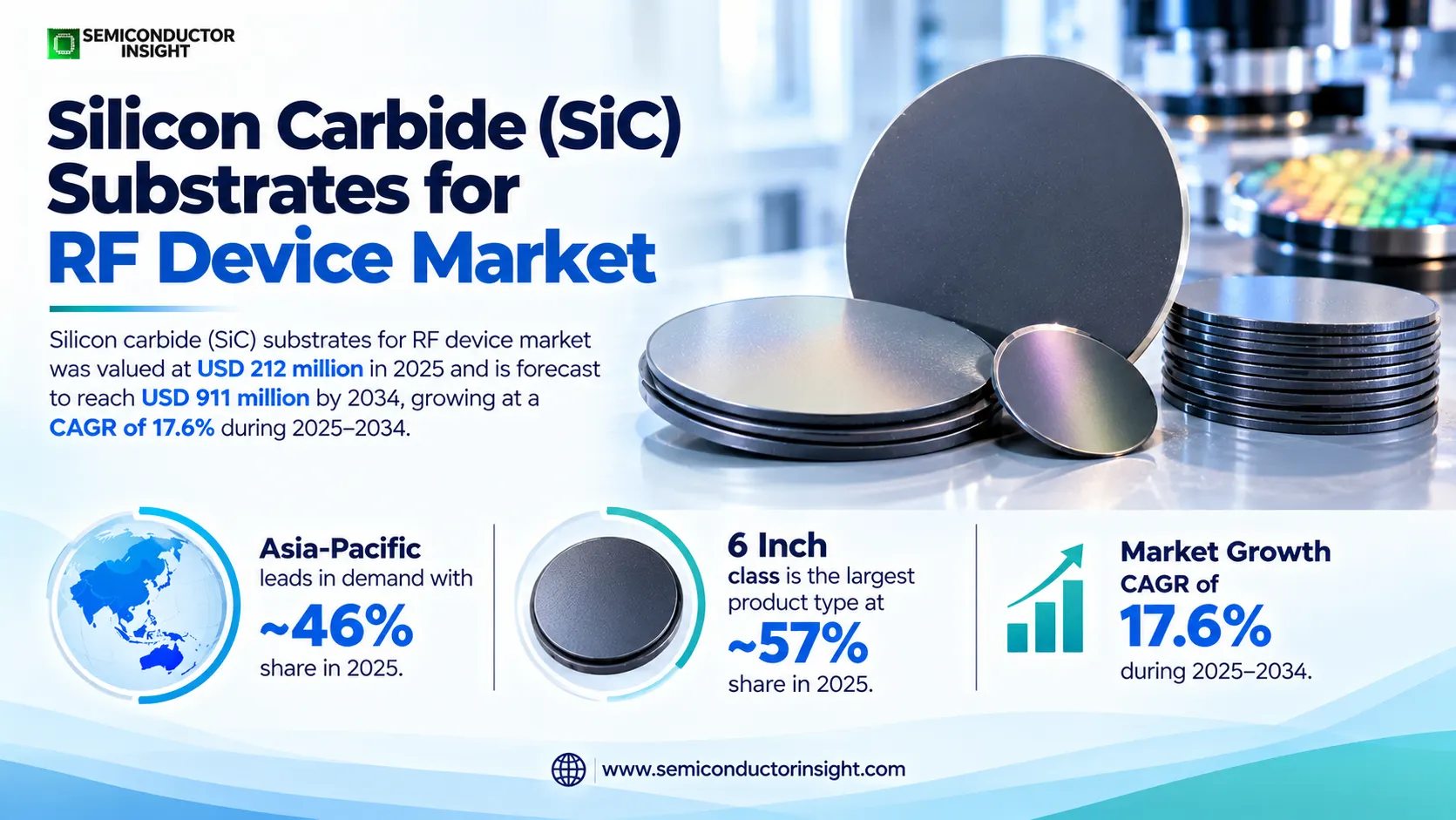
Silicon carbide (SiC) substrates for RF device market was valued at USD 212 million in 2025 and is forecast to reach USD 911 million by 2034, growing at a CAGR of 17.6% during 2025–2034. Asia-Pacific is the leading demand region, with an estimated ~46% share in 2025, while the 6 Inch class is the largest product type at ~57%.
Radio-frequency semiconductor devices use semi-insulating silicon carbide as a high-resistivity foundation for gallium nitride transistor layers. The crystal carries heat away from dense amplifier structures without introducing the electrical leakage associated with conductive power-device wafers. This combination is valuable in high-frequency radio transmitters where power density, linearity and thermal stability determine whether a device can meet the radio equipment maker’s specifications across years of outdoor service.
The revenue boundary includes finished RF-qualified semi-insulating SiC substrate wafers in 4 Inch, 6 Inch and 8 Inch formats, whether supplied to commercial or development-stage RF fabrication programs. It excludes finished GaN transistors, packaged RF power amplifiers, complete cellular base stations, silicon carbide power-device substrates sold into inverter production and separately priced epitaxial processing. This boundary matters because the surrounding compound-semiconductor ecosystem is considerably larger than the bare wafer opportunity.
Material qualification is more restrictive than a nominal wafer diameter suggests. RF customers inspect resistivity, crystal polytype, dislocation density, micropipe incidence, surface finish and the behavior of epitaxial layers across the wafer. Wolfspeed specifies 100 mm and 150 mm high-purity semi-insulating 4H-SiC production grades, while Coherent advertises semi-insulating material up to 200 mm. These product offerings establish a real technical progression without proving identical shipment volumes across sizes.
Telecom radio deployment provides the clearest link between end-market demand and wafer orders. When network vendors increase amplifier power or add frequency bands, device makers need more qualified die area and a stable GaN-on-SiC process. The International Telecommunication Union reported that 5G reached 55% of the world’s population in 2025, indicating substantial scope for network densification even in markets where initial nationwide launches have already occurred.
The outlook combines growing RF bandwidth requirements with the slower economics of crystal production. Larger diameters can reduce processing cost per die only when usable wafer yield and epitaxial uniformity keep pace, and RF qualification can take longer than power-device line expansion. Supplier differentiation therefore centers on repeatable crystal quality, application-specific specifications and reliable delivery to a comparatively small set of RF wafer-processing customers.
Segment Analysis: By Type
By type, RF-grade SiC substrates are sold as 4 Inch, 6 Inch and 8 Inch wafers. The 6 Inch format leads with an estimated ~57% of 2025 value and ~18.1% annual growth; 8 Inch material is a smaller ~9% category but has the fastest modeled expansion of ~28.1% as large-diameter qualification progresses. The 4 Inch legacy and specialized segment retains a meaningful ~34% share.
| Type | Function | Market position |
|---|---|---|
| 4 Inch | The 100 mm format supports established GaN-on-SiC device lines, development programs and RF parts whose order volumes do not justify immediate transfer to larger wafers. Its smaller surface simplifies some specialized process recipes and accommodates production equipment already amortized by device makers. Procurement decisions depend on stable resistivity and surface finish rather than a race toward maximum wafer diameter, particularly for lower-volume defense and industrial microwave applications. | Established share of ~34% in 2025; modeled ~11.7% CAGR. Existing epitaxial recipes and long device-qualification cycles keep the format commercially relevant even as leading telecom customers seek better wafer economics. Buyers value continuity of approved material grades, traceable crystal lots and low risk of redesign. Its relative share declines as 150 mm and 200 mm programs absorb new investment, but the absolute requirement for qualified small wafers can continue to rise. |
| 6 Inch | A 150 mm semi-insulating SiC wafer provides more die area per fabrication run while retaining an industrial supply base with explicit RF-grade specifications. Device manufacturers can spread lithography, deposition and inspection costs over a larger surface than on 100 mm material, provided crystal defects and epitaxial thickness variation remain controlled. Wolfspeed offers a named 150 mm HPSI product grade with on-axis orientation and a specified resistivity threshold. | Largest type at ~57% of 2025 revenue; estimated ~18.1% CAGR. This class represents the current commercial balance between mature process tools and economically attractive die count. The primary competitive battleground is repeatable yield across successive lots, not the largest demonstration wafer. Volume qualification by GaN amplifier manufacturers and the ability to support multiple radio designs give established material suppliers an advantage over entrants offering samples without production consistency. |
| 8 Inch | The 200 mm class offers the prospect of greater output from each deposition and patterning cycle but demands improved boule growth, slicing, polishing and wafer-level uniformity. Coherent identifies semi-insulating material up to 200 mm, making the category technically credible, while the broader SiC industry is developing 200 mm processing ecosystems. For RF customers, process migration additionally requires verification of GaN epitaxy and high-frequency transistor performance across the expanded diameter. | Emerging ~9% share with the highest modeled ~28.1% CAGR. The attractive growth percentage begins from a limited qualified revenue base and should not be read as evidence of universal commercial conversion. Development grades and selected production programs can contribute sales before every customer completes full qualification. The greatest commercial upside lies in high-throughput telecom amplifier lines where higher usable die output can justify the engineering expense of a larger platform. |
Diameter economics and RF material specifications
The diameter comparison must be interpreted alongside substrate electrical grade. High-purity semi-insulating 4H-SiC is not interchangeable with n-type conductive power electronics material, and even two semi-insulating products can differ in dopant strategy and dislocation characteristics. Wolfspeed lists undoped HPSI grades with at least 10^8 ohm-centimeter resistivity, whereas Coherent publishes a separate semi-insulating specification. Customer qualification must test the particular device stack rather than infer equivalence from the common SiC label.
In this market, the 4 Inch class protects mature production programs, the 6 Inch class captures the bulk of near-term RF expansion and the 8 Inch class offers the largest prospective unit-cost improvement. The modeled shares of ~34%, ~57% and ~9% respectively describe the revenue mix, not shipment counts. Price per wafer and the percentage of usable epitaxial area differ substantially across grades, so a volume-only comparison would misrepresent the economic position of each diameter.
Segment Analysis: By Application
Applications comprise 5G Base Station, Lidar and Others. Cellular RF amplifier demand holds the largest estimated ~69% of 2025 revenue, followed by miscellaneous microwave electronics at ~19% and LiDAR at ~12%. Base-station material value is expected to increase at ~18.4% annually, with the mix determined by amplifier power and substrate qualification rather than the headline number of mobile subscribers alone.
| Application | Demand characteristics |
|---|---|
| 5G Base Station | Leading application, ~69% share and modeled ~18.4% CAGR. GaN-on-SiC power amplifiers enable high-output radio units to handle wide channels, complex modulation and dense antenna arrays without excessive heat accumulation. Substrate orders follow the qualification of amplifier die for individual radio platforms, and network densification can increase RF material demand even where subscriber growth moderates. Device makers weigh crystal uniformity and thermal performance against the expense of premium semi-insulating grades. |
| Lidar | Specialized ~12% share with ~14.2% modeled growth. High-frequency electronics used in selected LiDAR transmit and receive systems can benefit from rugged compound-semiconductor platforms, although the majority of optical sensor architectures do not necessarily require GaN-on-SiC RF substrates. The commercial opportunity is consequently narrower than the total automotive or industrial LiDAR market. Qualification depends on reliability under temperature cycling, package integration and the particular microwave circuit topology. |
| Others | Residual ~19% share and ~16.5% modeled CAGR. This group captures defense radar, satellite communications, microwave infrastructure and specialized RF test or industrial equipment where power handling and thermal margins are important. Procurement is typically project-based and subject to long design lifetimes, making wafer consistency and traceability more decisive than low unit price. Small orders can still generate meaningful value because specialized crystal grades command higher qualification effort. |
The application structure separates recurring radio-platform programs from bespoke high-reliability contracts. A telecommunications amplifier wafer can be ordered repeatedly once a radio design enters production, while radar and industrial microwave demand may arrive in smaller qualification-led lots. These distinct purchasing cycles shape supplier inventories, engineering support and the proportion of development material sold alongside standard production grades. The segmentation does not include revenue from complete radios or optical sensor systems.
Regional Analysis
Asia-Pacific holds the largest estimated regional position at ~46% of 2025 RF substrate revenue and the strongest modeled ~19.0% CAGR. North America follows at ~26% with ~16.4% growth, while Europe contributes ~19% and advances at ~16.7%. South America (~4%) and the Middle East & Africa (~5%) are smaller markets in which radio-network expansion does not always translate into locally sourced substrate procurement.
Why do RF-grade silicon carbide substrate demand patterns differ by region?
The geographic split reflects a combination of where RF devices are designed, where crystals and epitaxial wafers are manufactured, and where the finished amplifiers are installed. Asia-Pacific benefits from high-volume telecommunications equipment supply chains; North America concentrates proprietary material technology and defense applications; Europe is shaped by integrated semiconductor manufacturing and supplier qualification. South America depends heavily on imported radio systems, while Gulf and African deployments create selective microwave equipment demand rather than large local crystal-fabrication bases.
| Region | Position | Growth outlook | Demand profile | What decides supplier selection |
|---|---|---|---|---|
| Asia-Pacific | Largest (~46%) | Highest (~19.0% CAGR) | Manufacturing and telecom demand | Local material qualification, radio-platform volume and cost per usable die |
| North America | Second (~26%) | Strong (~16.4% CAGR) | Materials innovation and defense | High-purity grades, technology transfer and supply assurance |
| Europe | Third (~19%) | Steady (~16.7% CAGR) | Integrated semiconductor investment | Long-term process stability and supplier certification |
| South America | Smaller (~4%) | Emerging (~14.0% CAGR) | Imported network equipment | Operator rollout timing and landed component cost |
| Middle East & Africa | Developing (~5%) | Selective (~15.8% CAGR) | Telecom and specialized microwave | Harsh-climate performance and regional project execution |
RF Silicon Carbide Substrate Manufacturers and Competitive Landscape
Competition is concentrated among material specialists that can supply high-resistivity crystals with documented surface and defect specifications. Wolfspeed and Coherent publish direct RF-grade semi-insulating product information, while several other semiconductor and crystal companies have broader SiC exposure that must be assessed separately from RF qualification. A buyer’s switching cost is high because the substrate influences epitaxial behavior and the yield of every subsequent microwave device fabrication step.
Wolfspeed differentiates its RF material offering with explicitly catalogued 4H-SiC high-purity semi-insulating wafers and associated GaN epitaxy capability. The company specifies production-grade substrates in 100 mm and 150 mm diameters, including orientation, thickness, resistivity and polished surface conditions. This level of detail is commercially significant because a device fab can design incoming inspection around measurable parameters and qualify a reproducible material supply, rather than accepting a general statement that a vendor makes silicon carbide.
Coherent competes through large-diameter semi-insulating material development and an integrated materials portfolio. Its RF electronics specification includes diameters up to 200 mm, with published thermal and electrical characteristics. Device makers assessing the 8 Inch class must still confirm lot-to-lot uniformity, epitaxial compatibility and economic yield. The supplier’s general SiC expansion announcements describe a broader industrial platform; they should not be read as direct evidence that all newly available wafer capacity is allocated to RF applications.
Corporate identities in historical supplier lists require careful treatment. Cree’s silicon carbide materials activities are associated with Wolfspeed, and the II-VI Advanced Materials identity is now represented under Coherent. STMicroelectronics completed its acquisition of Norstel in 2019, while ROHM’s SiCrystal business belongs to the wider ROHM group. These relationships affect the count of independent competitors and make it inappropriate to assign separate current market shares to former names and their owners.
Several Asian crystal suppliers are relevant to the broader SiC materials landscape, but a manufacturer’s ability to produce conductive power wafers does not establish a current commercial RF-grade HPSI product. SICC Materials, TankeBlue Semiconductor and other specialists should be evaluated against available technical specifications and direct customer qualifications before being treated as equivalent to suppliers publishing RF materials catalogs. Competitive position depends on usable wafer area, resistivity uniformity, crystal defects and dependable long-term deliveries, not just nominal boule diameter.
Tier structure
| Tier | Companies | Basis of competition |
|---|---|---|
| RF-qualified product suppliers | Wolfspeed; Coherent | Both companies publish dedicated semi-insulating SiC specifications for RF electronics and have identifiable material products, which makes their commercial RF relevance directly verifiable. Customers can compare resistivity, crystal form, wafer size and polishing characteristics when selecting substrates for GaN epitaxy. Their competitive advantage rests on process knowledge and qualification continuity, although public product specifications alone do not quantify their share of total market revenue. |
| Integrated semiconductor ecosystems | STMicroelectronics; ROHM | These groups possess silicon carbide manufacturing and device expertise, including acquired or subsidiary material operations. Their role in the RF substrate market must be distinguished from the larger conductive SiC power-device supply chain. Integration can support research, process transfer and security of supply, but individual RF-grade wafer sales require product-level evidence. They are therefore treated as strategically relevant participants rather than assigned unsupported leadership rankings. |
| Emerging crystal-material participants | SICC Materials; TankeBlue Semiconductor | Companies associated with silicon carbide crystal production may participate in customer qualification and specialized wafer development, but publicly available generic SiC descriptions do not prove the same HPSI product breadth as a dedicated RF catalog. For these businesses, the main opportunity is to demonstrate electrical isolation, surface preparation and defect control at a cost attractive to RF device makers. Their position remains dependent on verified application-specific specifications and repeat production orders. |
Key companies profiled
- Wolfspeed (United States)
- Coherent (United States)
- STMicroelectronics (Europe)
- ROHM / SiCrystal (Japan / Germany)
- SICC Materials (China)
- TankeBlue Semiconductor (China)
RF-Grade Silicon Carbide Substrate Production and Capacity Analysis
RF-grade substrate production starts with high-purity crystal growth and continues through boule slicing, grinding, polishing, defect mapping and electrical qualification. A factory capable of producing conductive SiC wafers for inverters cannot automatically supply semi-insulating material for microwave electronics. The capacity constraint is therefore the amount of qualified, usable RF wafer area delivered to device makers, not the gross number of silicon carbide crystals grown across the industry.
Crystal growth determines whether the eventual substrate achieves the resistivity and crystalline quality required for GaN RF transistors. Suppliers control impurities, dopant behavior, crystal orientation and defect formation during a long thermal process, then remove damaged material during slicing and polishing. Wolfspeed’s published 100 mm and 150 mm HPSI grades demonstrate the specification burden: orientation and resistance are documented alongside the surface condition required for epitaxial deposition. A yield loss at any of these stages raises the effective price of each usable wafer.
Larger diameter technology can change economics without immediately increasing qualified shipments. Coherent’s 200 mm semi-insulating offering shows that an 8 Inch RF route exists, while a separate 2024 epitaxial capacity announcement describes broader SiC manufacturing investments. The area advantage is attractive only if a high fraction of the wafer meets the device maker’s electrical and epitaxial criteria. For RF products, uniformity of GaN layers and microwave performance after fabrication can be more limiting than the ability to cut a larger crystal.
The industry’s most visible advanced diameter milestone is a 300 mm single-crystal SiC demonstration, but that wafer size sits beyond the three commercial diameter categories used here. Demonstration progress is relevant to future process scaling and materials research rather than a reason to count 300 mm RF wafer revenue in the current outlook. The production model consequently prioritizes present customer-qualified 100 mm and 150 mm supply, measured 200 mm development and the slow transfer of successful process recipes between wafer platforms.
RF Silicon Carbide Substrate Market Dynamics: Drivers, Restraints and Opportunities
Demand increases as cellular transmitters require greater RF power density, as GaN-on-SiC amplifiers penetrate additional microwave applications and as wafer makers improve the yield of larger diameters. Countervailing forces include expensive crystal growth, qualification delays, defects and competition from alternative RF material platforms. The impact contributions below are modeled commercial influences on the forecast, not measured shares of any single company or network deployment program.
MARKET DRIVERS
Drivers Impact Analysis*
| Market Drivers | Impact Rank | CAGR Contribution (%) | 2026–2028 | 2029–2031 | 2032–2034 |
|---|---|---|---|---|---|
| Higher power density in 5G radio amplifiers | High | +6.20% | High | High | Medium |
| 150 mm RF substrate qualification and yield gains | High | +5.40% | High | High | Medium |
| 200 mm development and process transfer | Medium-High | +4.10% | Low | High | High |
| Defense and satellite microwave electronics | Medium | +3.20% | Medium | Medium | High |
| Growth in specialized RF and industrial sensing | Low-Medium | +2.10% | Low | Medium | High |
| Others (materials engineering and supply diversification) | Low | +1.20% | Medium | Medium | Medium |
RF power density supports premium substrates
Massive-MIMO radio systems and wider carrier bandwidth create amplifier designs in which thermal resistance and electrical isolation materially affect performance. GaN-on-SiC can support high power operation where the equipment maker values efficiency and compact cooling. The substrate represents only one layer of the device value chain, but its crystal quality influences epitaxial defects and therefore the usable yield of costly RF transistors. This encourages repeat purchases of proven grades after qualification.
150 mm adoption improves manufacturing economics
A move from 100 mm to 150 mm wafers increases nominal processing area, allowing the same fabrication sequence to produce more devices when yield is maintained. The transition is commercially meaningful because many RF manufacturers already possess mature smaller-wafer recipes and need evidence that the larger surface performs consistently. Supplier catalogs with production-grade 150 mm specifications help shorten technical evaluation, but process transfer still requires measurement of RF device performance rather than reliance on geometric area alone.
Larger diameter development broadens the addressable base
Coherent’s stated availability of semi-insulating SiC up to 200 mm creates a pathway for customers considering higher-throughput microwave fabrication. The immediate market opportunity includes engineering wafers, pilot lots and process characterization before full production migration. A supplier that demonstrates low defect density across a larger surface can win long-lived material positions when device makers redesign their lines. Conversely, poor epitaxial uniformity can erase the cost benefit of increased wafer diameter.
High-reliability microwave applications diversify demand
Radar, aerospace and satellite communications equipment can require sustained RF output under demanding thermal and environmental conditions. These programs may consume fewer wafers than mass-market cellular equipment but often place greater weight on material traceability, device reliability and predictable specification compliance. RF-grade semi-insulating substrates support this product class where GaN technology is selected, giving suppliers a demand stream less directly tied to mobile operator capital expenditure cycles.
MARKET RESTRAINTS
Restraints Impact Analysis*
| Market Restraints | Impact Rank | CAGR Contribution (%) | 2026–2028 | 2029–2031 | 2032–2034 |
|---|---|---|---|---|---|
| Crystal growth and RF-grade wafer costs | High | -1.90% | High | High | Medium |
| Qualification time and epitaxial yield risk | Medium-High | -1.40% | High | Medium | Medium |
| Alternative RF material platforms | Medium | -0.80% | Medium | Medium | High |
| Others (program delays and limited specialized capacity) | Low | -0.50% | Medium | Low | Medium |
Semi-insulating crystal quality remains costly
Growing a high-resistivity crystal suitable for microwave electronics requires tight control of impurities and defects over a substantial thermal processing cycle. Subsequent wafer preparation must achieve the flatness and surface condition needed for epitaxy. When customers reject wafers for local defects or inconsistent resistivity, the effective cost of usable material rises rapidly. These quality demands make the RF substrate market less price-elastic than generic silicon wafers and slow entry by unqualified suppliers.
Device makers must validate every platform change
A new wafer supplier or diameter can alter GaN epitaxial behavior, transistor yield and long-term RF performance. Customers therefore require extensive electrical and reliability data before converting a production radio amplifier to another substrate grade. This qualification burden protects incumbent vendors but delays the commercialization of larger-wafer innovations. It also means that announcing a new crystal diameter does not guarantee immediate material revenue, particularly in high-reliability defense and infrastructure programs.
Competing RF semiconductors retain selected sockets
Silicon LDMOS, GaAs and GaN-on-silicon technologies remain alternatives in different power, frequency and cost envelopes. A radio equipment designer chooses the complete amplifier architecture rather than the substrate in isolation, and not every additional 5G radio requires a semi-insulating SiC wafer. This substitution risk limits the proportion of network investment captured by the RF SiC material segment even as total radio traffic and spectrum usage increase.
Investment cycles can defer specialized orders
Telecommunications capital spending is uneven, while aerospace and defense programs often depend on qualification milestones and government procurement. A wafer supplier may face pauses between customer pilot lots and sustained orders even when technical evaluations are successful. Limited specialist manufacturing capacity can compound these fluctuations because high-purity crystal lines cannot be scaled instantly. The result is a market in which order timing and revenue recognition may differ from the steady long-term technology adoption curve.
MARKET OPPORTUNITIES
RF-specific 200 mm process qualification
Suppliers that can provide repeatable 200 mm semi-insulating material with strong GaN epitaxial uniformity can help device makers reduce cost per amplifier die. The opportunity is not merely to advertise a larger diameter but to deliver stable resistance, low defect density and predictable yield at commercial lot sizes. Successful qualification could open multi-year supply contracts for high-volume radio components and specialized microwave circuits, expanding the market without counting unrelated conductive SiC capacity.
Trusted sourcing for defense electronics
National security and aerospace procurement can favor documented provenance and reliable access to critical RF materials. A supplier with transparent crystal-growth control, lot-level characterization and established quality systems may earn a premium over a lower-cost vendor lacking the required traceability. Such contracts are smaller in unit volume than consumer electronics but can support durable material demand and technology development that later improves commercial telecommunications wafer quality.
Material and epitaxy partnerships
A semi-insulating wafer’s commercial value is realized when GaN epitaxial layers and RF transistors achieve stable performance on it. Collaboration between crystal growers, epitaxy houses and amplifier designers can reduce the number of qualification iterations and accelerate new diameter introductions. Suppliers able to provide matched material characterization and device-process support may capture more customer programs than those competing solely on wafer price, while keeping epitaxy service revenue outside the defined bare-substrate market.
Emerging-market network capacity upgrades
Where cellular networks are moving from initial coverage toward higher-capacity operation, amplifier designers have incentives to reduce thermal losses and increase output power per radio unit. That can create additional demand for GaN-on-SiC substrate material even if the number of physical sites grows slowly. The commercial opportunity depends on specific radio architectures and chip sourcing, so it is best pursued through equipment makers and RF semiconductor fabs rather than inferred directly from national 5G population coverage.
RF Silicon Carbide Substrate Supply Chain Analysis
The value chain begins with ultra-high-purity SiC feedstock and crystal growth, passes through wafer finishing and electrical characterization, and reaches GaN epitaxy and RF transistor fabrication before integration into amplifiers and communications equipment. The substrate supplier captures value through defect control and repeatability; device makers capture value through transistor design and fabrication. Separating these stages prevents double counting of wafer, epitaxy, device and system revenue.
Crystal feedstock and growth. RF material production starts with feedstock purity and tightly controlled crystal growth. The selected crystal polytype, impurity profile and defect population affect the substrate’s suitability for high-frequency GaN transistors. Specialized growth equipment and characterization methods create barriers to rapid capacity additions, and a low-cost boule is not necessarily economical if wafer yield is poor. Material vendors therefore invest heavily in process consistency and retain customers through the reproducibility of their crystal specifications.
Wafer preparation and inspection. After growth, boules are sliced and finished into epitaxy-ready substrates with demanding surface and dimensional tolerances. Inspection includes defects, resistivity, orientation and surface roughness, because small irregularities can impair the later GaN film and microwave device yield. The wafer preparation stage is particularly important during a transition from 100 mm to 150 mm or 200 mm, when process equipment and uniformity requirements change. Qualified inspection records provide customers with evidence of material reliability.
GaN device processing. Epitaxy companies and RF semiconductor fabs deposit nitride layers on the semi-insulating SiC wafer and then form high-frequency transistor structures. The bare substrate becomes one input to a substantially more valuable finished RF device, so the device maker’s revenue must not be treated as substrate sales. Technical feedback from epitaxial and transistor testing nevertheless determines which material supplier wins future contracts, making collaborative yield improvement a central part of substrate commercialization.
Equipment procurement. Radio equipment and aerospace system manufacturers select amplifiers for performance, reliability, supply assurance and cost. They generally buy devices or packaged modules rather than bare SiC wafers, but their platform choices determine upstream material demand. Long design cycles can lock in a substrate source for years, while a major radio redesign may trigger a new qualification opportunity. Suppliers with dependable delivery and transparent technical support can benefit from these procurement structures even without selling directly to network operators.
Recent Developments in RF-Grade Silicon Carbide Substrates
- 13 January 2026 Technology milestone
Wolfspeed reported producing a single-crystal 300 mm SiC wafer and described potential future uses across power, optical and RF platforms. The achievement is an important crystal-growth demonstration, but 300 mm RF substrates are not a fourth commercial type in this market. The practical significance is a longer-term technology path toward higher wafer throughput if subsequent high-purity semi-insulating specifications and device qualifications can be met. Source - 13 October 2026 Statistics published
The International Telecommunication Union released updated mobile-network coverage statistics showing that 5G reached 55% of the world population in 2025, with significant regional differences. This evidence provides demand context for high-performance RF electronics without converting telecom coverage into wafer revenue. Suppliers may benefit when capacity upgrades require GaN-on-SiC amplifiers, but actual substrate sales depend on device content and fab sourcing. Source - 16 June 2026 Industry outlook
Ericsson reported that 5G subscriptions exceeded three billion in the first quarter of 2026 and outlined continued adoption through 2031. Subscriber growth supports the commercial rationale for denser radio networks and advanced amplifier designs, while remaining several steps removed from RF substrate purchasing. Material producers should therefore use the outlook to evaluate future platform opportunities rather than treat mobile subscriptions as a direct wafer shipment forecast. Source - 2025 Manufacturing update
STMicroelectronics described developments in its silicon carbide manufacturing footprint and larger-wafer roadmap, including activity associated with Catania. The industrial investment expands the European SiC processing ecosystem and may generate transferable process knowledge. Most publicly discussed capacity relates to power electronics, however, so its existence does not establish an equivalent increase in RF-grade semi-insulating substrate production or immediate sales. Source - 26 September 2024 Capacity announcement
Coherent announced an expansion of silicon carbide epitaxial wafer production, discussing larger-diameter processing economics. Epitaxial wafer capacity is adjacent to the bare RF substrate category and should not be booked as identical revenue. The significance for material suppliers is improved experience with larger wafers, which may help future GaN-on-SiC RF qualification when suitable semi-insulating crystal quality is available. Source - 2 December 2019 Ownership update
STMicroelectronics completed its acquisition of Norstel, a silicon carbide wafer specialist, bringing the business under the larger semiconductor group. The event remains relevant when interpreting historical lists of substrate suppliers, since the two names should not be counted as unrelated current competitors. Ownership integration may support wafer technology investment, but RF-specific market position still depends on verified products and customer qualifications. Source
REPORT SCOPE & SEGMENTATION
| Attribute | Details |
|---|---|
| Market Size 2025 | USD 212 million |
| Estimated Size 2026 | USD 249 million |
| Forecast Size 2034 | USD 911 million |
| Growth Rate | CAGR of 17.6% from 2025–2034 |
| Unit | Value in USD million; semi-insulating RF substrate wafers |
| Historical Reference | 2023 publisher monetary anchor; 2025 modeled base |
| By Type | 4 Inch · 6 Inch · 8 Inch |
| By Application | 5G Base Station · Lidar · Others |
| By Region | Regional comparisons include modeled shares and growth for five geographic groups, with country-level commercial drivers. North AmericaUnited States, Canada, Mexico EuropeItaly, Germany, France, United Kingdom, Nordic countries, Rest of Europe Asia-PacificChina, Japan, South Korea, India, Southeast Asia, Rest of Asia-Pacific South AmericaBrazil, Argentina, Chile, Colombia, Rest of South America Middle East & AfricaSaudi Arabia, UAE, South Africa, Rest of Middle East and Africa |
| Key Companies Profiled | Wolfspeed, Coherent, STMicroelectronics, ROHM / SiCrystal, SICC Materials, TankeBlue Semiconductor |
| Customization Scope | Country, diameter and RF application scope can be customized through a client-specific research engagement. |
Frequently Asked Questions
What is the size and growth outlook for RF silicon carbide substrates?
The global market is valued at USD 212 million in 2025 and projected to reach USD 911 million in 2034, equivalent to a 17.6% CAGR over 2025–2034. An intermediate estimate of USD 249 million for 2026 reflects growing GaN-on-SiC amplifier demand. The figures concern bare semi-insulating RF-qualified substrate wafers, not packaged RF devices or complete mobile radio systems.
What makes a SiC substrate suitable for RF electronics?
An RF-grade wafer combines high electrical resistivity with good thermal conduction and a crystal surface appropriate for GaN epitaxy. The isolation helps limit unwanted electrical leakage, while heat dissipation supports high-output microwave transistor operation. Device manufacturers also assess crystal defects, orientation and the consistency of material properties across the wafer. These requirements distinguish RF semi-insulating grades from conductive SiC substrates used for power MOSFETs.
Which substrate diameter accounts for the largest share?
The 6 Inch or 150 mm class leads with an estimated ~57% of market revenue, reflecting a useful balance between established manufacturing tools and wafer processing area. The 4 Inch class retains ~34% through mature and specialized device programs. The 8 Inch format represents ~9% and is the fastest-growing category at a modeled ~28.1% CAGR, but larger-wafer availability does not imply universal customer qualification.
Which end-use application generates the most demand?
5G base-station RF amplifiers account for an estimated ~69% of the substrate revenue mix because selected GaN-on-SiC devices provide high power density and thermal stability for radio units. LiDAR contributes a modeled ~12%, while radar, satellite communications and other microwave uses represent ~19%. These are analytical allocations of wafer value, not shares of all telecommunications or sensing equipment spending.
Where is the leading regional market for RF SiC substrates?
Asia-Pacific leads with an estimated ~46% share and modeled ~19.0% annual growth, supported by radio equipment manufacturing, semiconductor processing and large network upgrades. North America holds about ~26%, with strength in materials technology and specialized electronics, while Europe contributes ~19%. The smaller regions generally access RF substrate technology through imported semiconductor components rather than extensive local crystal production.
How do Wolfspeed and Coherent compete in RF materials?
The two suppliers approach microwave device customers through differentiated crystal characterization and technical support. Wolfspeed details polished epitaxy-ready HPSI production grades, whereas Coherent emphasizes high-resistivity material and the progression toward larger RF wafer formats. Selection depends on the transistor fab’s own incoming-material measurements, epitaxial process results and yield history. A diameter label by itself is insufficient to establish suitability for a particular GaN amplifier design.
Why is 200 mm RF wafer adoption commercially important?
An 8 Inch wafer offers more geometric area than a 6 Inch wafer and can improve device output per fabrication run when usable yield remains high. The transition requires suitable crystal quality, epitaxial uniformity and compatible process tools, so development shipments may precede full-volume conversion. The strongest commercial benefit arises in qualified high-throughput RF lines where the higher area offsets migration costs and wafer-grade price premiums.
What are the principal risks to this market?
High-purity crystal production is expensive, and defects or nonuniform resistivity can reduce the amount of saleable RF material. Customer qualification can take substantial time, especially when changing diameter or supplier. Competing semiconductor platforms also retain certain radio-frequency applications, while telecom capital expenditure cycles can defer device programs. These factors create a slower and less predictable revenue ramp than a simple projection of global 5G subscriber growth would suggest.
Are power-device SiC substrates included in the forecast?
No. Conductive substrates sold for electric-vehicle inverters, chargers and industrial power MOSFETs are outside the RF-grade semi-insulating substrate boundary. The scope also excludes finished GaN transistors, packaged amplifiers and separately priced epitaxial services. Some manufacturers participate in both material categories, and their corporate investment announcements can be relevant technology context without being counted as RF wafer revenue.
What are the geographic and product segments covered?
The study covers North America, Europe, Asia-Pacific, South America and the Middle East and Africa, with modeled regional shares and selected country demand drivers. Its product segmentation follows three wafer diameters—4 Inch, 6 Inch and 8 Inch—and three applications: 5G Base Station, Lidar and Others. The 2025 base, 2026 estimate and 2034 forecast provide a consistent revenue framework for these segments.
Research Sources & Evidence Base
Get Sample Report PDF for Exclusive Insights
Report Sample Includes
- Table of Contents
- List of Tables & Figures
- Charts, Research Methodology, and more...
 Download Sample Report PDF