Semiconductor Wafer Polishing Pad Market Overview
Semiconductor Wafer Polishing Pad is a product which increases semiconductor integration by smoothening the semiconductor wafer surface through physical and chemical polishing processes.
This report provides a deep insight into the global Semiconductor Wafer Polishing Pad market covering all its essential aspects. This ranges from a macro overview of the market to micro details of the market size, competitive landscape, development trend, niche market, key market drivers and challenges, SWOT analysis, value chain analysis, etc.
The analysis helps the reader to shape the competition within the industries and strategies for the competitive environment to enhance the potential profit. Furthermore, it provides a simple framework for evaluating and accessing the position of the business organization. The report structure also focuses on the competitive landscape of the Global Semiconductor Wafer Polishing Pad Market, this report introduces in detail the market share, market performance, product situation, operation situation, etc. of the main players, which helps the readers in the industry to identify the main competitors and deeply understand the competition pattern of the market.
In a word, this report is a must-read for industry players, investors, researchers, consultants, business strategists, and all those who have any kind of stake or are planning to foray into the Semiconductor Wafer Polishing Pad market in any manner.
Semiconductor Wafer Polishing Pad Market Analysis:
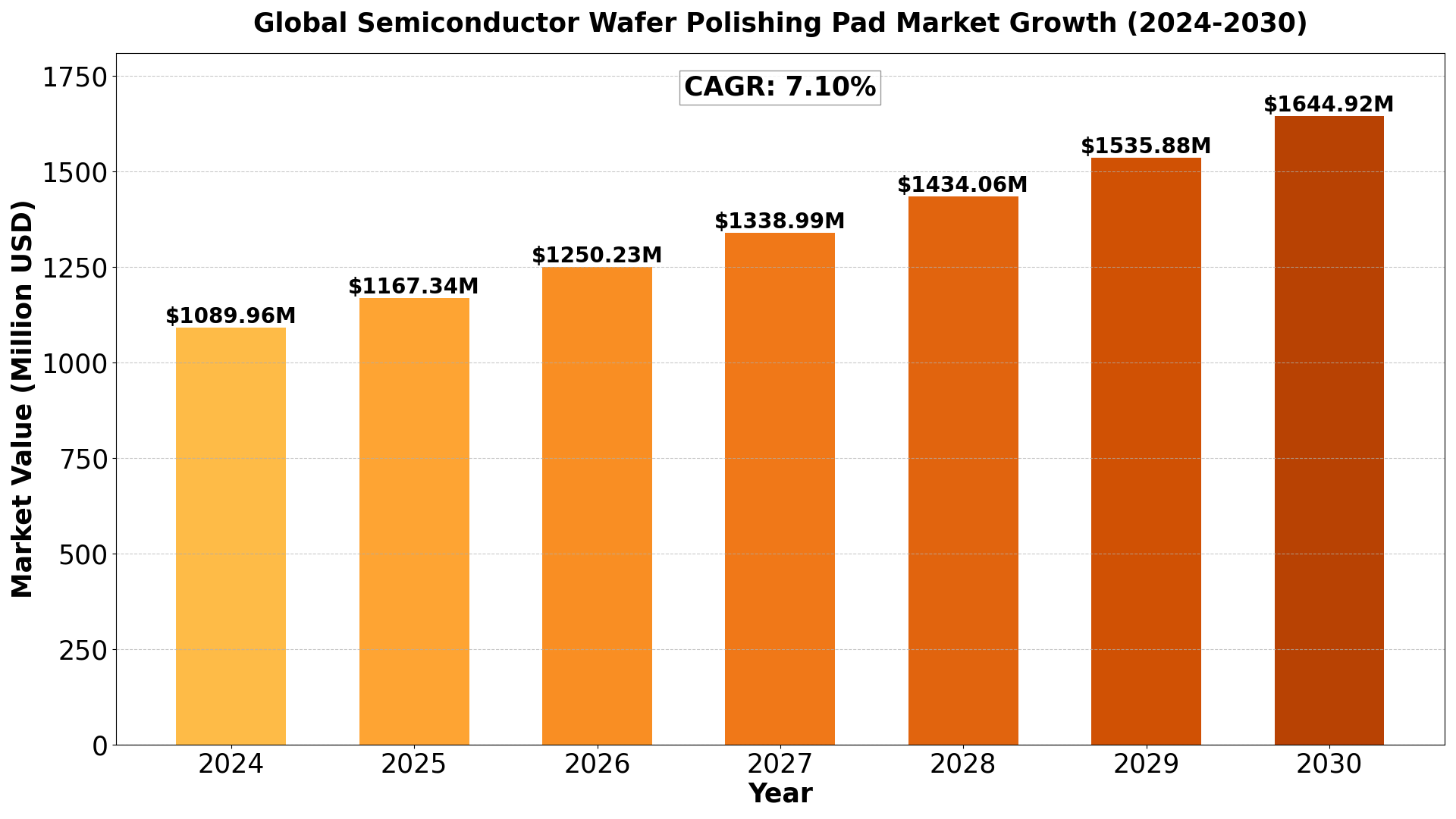
The Global Semiconductor Wafer Polishing Pad Market size was estimated at USD 1017.70 million in 2023 and is projected to reach USD 1644.92 million by 2030, exhibiting a CAGR of 7.10% during the forecast period.
North America Semiconductor Wafer Polishing Pad market size was USD 265.18 million in 2023, at a CAGR of 6.09% during the forecast period of 2024 through 2030.
Semiconductor Wafer Polishing Pad Key Market Trends :
- Demand for Advanced Semiconductor Devices: With the growing demand for high-performance and miniaturized semiconductor devices for applications in 5G, AI, IoT, and automotive electronics, there is an increasing need for precise wafer polishing during semiconductor fabrication. Polishing pads are crucial for achieving the required smoothness and flatness of wafers, especially as the size of semiconductor nodes continues to shrink.
- Advancements in Wafer Polishing Technology: New developments in wafer polishing technology, including improvements in polishing pad materials and design, are driving the market. Innovations such as advanced slurry-free polishing techniques, diamond-like carbon (DLC) coatings, and the development of more efficient pads with better durability are improving the performance and efficiency of the polishing process, meeting the stringent requirements of next-generation semiconductor manufacturing.
- Focus on Yield and Quality Enhancement: As semiconductor manufacturers focus on improving yields and reducing defects, polishing pads play a critical role in ensuring the uniformity and smoothness of wafer surfaces. High-quality polishing pads contribute to reducing wafer defects and scratches, which in turn enhances the overall yield and performance of semiconductor devices. This need for higher-quality, defect-free wafers is a key driver of demand for wafer polishing pads.
- Increasing Automation in Semiconductor Manufacturing: The rise of automation in semiconductor manufacturing processes is influencing the demand for more precise and consistent polishing pads. Automated systems require reliable and high-performance polishing materials that ensure consistent wafer quality across high-volume production lines. The integration of polishing pads into automated wafer processing equipment is a growing trend, driving the market for innovative polishing solutions.
- Sustainability and Environmental Considerations: As the semiconductor industry places greater emphasis on sustainability, the demand for environmentally friendly and recyclable polishing pads is rising. Manufacturers are focusing on creating pads that reduce waste, have longer lifecycles, and are made from sustainable materials. These eco-friendly pads are helping semiconductor producers reduce their environmental impact while maintaining the required performance in the polishing process.
Semiconductor Wafer Polishing Pad Market Regional Analysis :

1. North America (USA, Canada, Mexico)
- USA: The largest market in the region due to advanced infrastructure, high disposable income, and technological advancements. Key industries include technology, healthcare, and manufacturing.
- Canada: Strong market potential driven by resource exports, a stable economy, and government initiatives supporting innovation.
- Mexico: A growing economy with strengths in automotive manufacturing, agriculture, and tourism, benefitting from trade agreements like the USMCA.
2. Europe (Germany, UK, France, Russia, Italy, Rest of Europe)
- Germany: The region’s industrial powerhouse with a focus on engineering, automotive, and machinery.
- UK: A hub for financial services, fintech, and pharmaceuticals, though Brexit has altered trade patterns.
- France: Strong in luxury goods, agriculture, and aerospace with significant innovation in renewable energy.
- Russia: Resource-driven economy with strengths in oil, gas, and minerals but geopolitical tensions affect growth.
- Italy: Known for fashion, design, and manufacturing, especially in luxury segments.
- Rest of Europe: Includes smaller yet significant economies like Spain, Netherlands, and Switzerland with strengths in finance, agriculture, and manufacturing.
3. Asia-Pacific (China, Japan, South Korea, India, Southeast Asia, Rest of Asia-Pacific)
- China: The largest market in the region with a focus on technology, manufacturing, and e-commerce. Rapid urbanization and middle-class growth fuel consumption.
- Japan: Technological innovation, particularly in robotics and electronics, drives the economy.
- South Korea: Known for technology, especially in semiconductors and consumer electronics.
- India: Rapidly growing economy with strengths in IT services, agriculture, and pharmaceuticals.
- Southeast Asia: Key markets like Indonesia, Thailand, and Vietnam show growth in manufacturing and tourism.
- Rest of Asia-Pacific: Emerging markets with growing investment in infrastructure and services.
4. South America (Brazil, Argentina, Colombia, Rest of South America)
- Brazil: Largest economy in the region, driven by agriculture, mining, and energy.
- Argentina: Known for agriculture exports and natural resources but faces economic instability.
- Colombia: Growing economy with strengths in oil, coffee, and flowers.
- Rest of South America: Includes Chile and Peru, which have strong mining sectors.
5. The Middle East and Africa (Saudi Arabia, UAE, Egypt, Nigeria, South Africa, Rest of MEA)
- Saudi Arabia: Oil-driven economy undergoing diversification with Vision 2030 initiatives.
- UAE: Financial hub with strengths in tourism, real estate, and trade.
- Egypt: Growing infrastructure development and tourism.
- Nigeria: Largest economy in Africa with strengths in oil and agriculture.
- South Africa: Industrialized economy with strengths in mining and finance.
- Rest of MEA: Includes smaller yet resource-rich markets like Qatar and Kenya with growing infrastructure investments.
Semiconductor Wafer Polishing Pad Market Segmentation :
The research report includes specific segments by region (country), manufacturers, Type, and Application. Market segmentation creates subsets of a market based on product type, end-user or application, Geographic, and other factors. By understanding the market segments, the decision-maker can leverage this targeting in the product, sales, and marketing strategies. Market segments can power your product development cycles by informing how you create product offerings for different segments.
Key Company
- DuPont
- CMC Materials
- FUJIBO
- IVT Technologies
- SKC
- Hubei Dinglong
- TWI Incorporated
- 3M
- FNS TECH
- KPX
- Hard Pad
- Soft Pad
- 300 mm Wafer
- 200 mm Wafer
- Others
Drivers
- Increasing Demand for Advanced Semiconductors: The growing demand for high-performance semiconductors in various applications such as consumer electronics, telecommunications, automotive, and IoT has driven the need for efficient wafer polishing. As semiconductor devices become smaller and more complex (e.g., 5nm and 3nm nodes), precise wafer polishing is critical to meet the required standards.
- Miniaturization of Semiconductor Devices: The ongoing trend towards miniaturization of semiconductor devices necessitates ultra-thin wafers and high-precision polishing to maintain the required flatness and smoothness. The demand for semiconductor wafer polishing pads increases as the process becomes more critical for smaller node devices.
- Expansion of Semiconductor Production in Emerging Markets: The increasing number of semiconductor fabs in emerging markets, particularly in Asia-Pacific (e.g., China, South Korea, Taiwan, and India), is driving the need for polishing pads. This expansion is largely due to the rising demand for electronic devices and the ongoing trend toward local semiconductor manufacturing.
- Advances in Semiconductor Packaging: Advanced packaging technologies, such as 3D packaging and fan-out wafer-level packaging (FOWLP), require highly precise wafer polishing to ensure effective integration of the semiconductor components. This drives demand for specialized polishing pads.
- Growth of Electric Vehicles (EVs): The automotive sector’s transition to electric vehicles (EVs) and the increased reliance on semiconductors for electric powertrains, battery management systems, and autonomous driving technologies contribute to the demand for wafer polishing pads. These technologies require highly efficient and reliable semiconductor components that undergo CMP for planarization.
- Development of Memory and Logic Chips: The growing demand for memory chips (e.g., DRAM and NAND) and logic chips (e.g., processors) for cloud computing, AI, and big data analytics further fuels the demand for wafer polishing pads, as these chips require high-quality planarization for optimal performance.
Restraints
- High Cost of Polishing Pads: Semiconductor wafer polishing pads are expensive, and the cost can be a significant barrier, particularly for smaller manufacturers or for those operating at lower production volumes. The high initial investment and recurring costs for polishing pads can impact the profitability of semiconductor fabrication.
- Wear and Tear of Polishing Pads: Wafer polishing pads wear out over time due to the abrasive nature of the CMP process. This wear and tear result in frequent replacements, adding to the operational costs for semiconductor manufacturers.
- Environmental Concerns: The CMP process uses chemical slurries in conjunction with polishing pads, and improper disposal of these chemicals can lead to environmental contamination. Manufacturers must adhere to stringent regulations regarding chemical waste management, which can add to the overall cost and complexity of operations.
- Technological Limitations: As semiconductor devices shrink and the demands for wafer precision increase, polishing pads must evolve to meet the stringent requirements. Not all existing polishing pads may be suitable for the latest technologies, leading to the need for continuous innovation in pad design and material composition.
- Supply Chain Challenges: The semiconductor industry has been grappling with supply chain disruptions, including shortages of raw materials and logistics challenges. This affects the availability of wafer polishing pads and can lead to production delays for semiconductor manufacturers.
Opportunities
- R&D and Innovation in Polishing Pads: There are significant opportunities for innovation in semiconductor wafer polishing pads. Manufacturers are developing pads with enhanced durability, lower wear rates, and superior performance to meet the evolving needs of smaller node semiconductors, advanced packaging technologies, and emerging semiconductor materials (e.g., gallium nitride, silicon carbide).
- Emerging Technologies in Semiconductor Devices: The development of new semiconductor technologies, such as AI chips, quantum computing chips, and high-performance computing processors, presents opportunities for specialized polishing pads. These devices require tailored polishing solutions to achieve the necessary flatness and quality for integration.
- Sustainability and Eco-Friendly Solutions: With growing concerns about environmental impact, there is an increasing demand for more sustainable polishing pads and eco-friendly alternatives. Pads made from recyclable materials or with reduced environmental impact during the polishing process present an opportunity for growth in the market.
- Expansion of Semiconductor Fabs in Emerging Economies: As semiconductor manufacturing continues to grow in emerging economies like India and Southeast Asia, the demand for wafer polishing pads is expected to rise. Establishing strong partnerships in these regions can provide significant growth opportunities.
- Customization for Specific Applications: With the increasing diversification of semiconductor applications, there is an opportunity for companies to develop customized polishing pads for specific use cases, such as memory chips, logic chips, power devices, and sensors. These customized solutions can provide manufacturers with a competitive edge.
- Increased Demand in 5G and Telecommunications: The expansion of 5G networks and the growing use of semiconductor-based components in telecommunications infrastructure create demand for highly efficient wafer polishing pads. Components used in communication devices need to meet high precision and performance standards, driving the market for polishing pads.
Challenges
- Rising Raw Material Costs: The cost of raw materials used to manufacture polishing pads, such as polyurethane, silica, and abrasives, is rising due to supply chain constraints and market fluctuations. These increasing costs may affect the pricing of polishing pads and put pressure on profit margins for manufacturers.
- Complexity of CMP Process: The complexity of the CMP process, especially for advanced semiconductor nodes (e.g., 7nm, 5nm, and below), requires polishing pads to provide high levels of precision and uniformity. Achieving this consistency can be challenging and resource-intensive for manufacturers.
- Intense Competition: The semiconductor wafer polishing pad market is highly competitive, with multiple players offering similar products. To stand out in the market, manufacturers must constantly innovate to provide pads that meet the specific needs of semiconductor manufacturers, including enhanced performance, longevity, and environmental sustainability.
- Integration with Advanced Manufacturing Systems: As semiconductor fabs adopt more automated and smart manufacturing systems, polishing pads must be compatible with these advanced systems. Ensuring compatibility with robotic systems and other automated equipment can be challenging and requires ongoing investment in R&D.
Key Benefits of This Market Research:
- Industry drivers, restraints, and opportunities covered in the study
- Neutral perspective on the market performance
- Recent industry trends and developments
- Competitive landscape & strategies of key players
- Potential & niche segments and regions exhibiting promising growth covered
- Historical, current, and projected market size, in terms of value
- In-depth analysis of the Semiconductor Wafer Polishing Pad Market
- Overview of the regional outlook of the Semiconductor Wafer Polishing Pad Market:
Key Reasons to Buy this Report:
- Access to date statistics compiled by our researchers. These provide you with historical and forecast data, which is analyzed to tell you why your market is set to change
- This enables you to anticipate market changes to remain ahead of your competitors
- You will be able to copy data from the Excel spreadsheet straight into your marketing plans, business presentations, or other strategic documents
- The concise analysis, clear graph, and table format will enable you to pinpoint the information you require quickly
- Provision of market value (USD Billion) data for each segment and sub-segment
- Indicates the region and segment that is expected to witness the fastest growth as well as to dominate the market
- Analysis by geography highlighting the consumption of the product/service in the region as well as indicating the factors that are affecting the market within each region
- Competitive landscape which incorporates the market ranking of the major players, along with new service/product launches, partnerships, business expansions, and acquisitions in the past five years of companies profiled
- Extensive company profiles comprising of company overview, company insights, product benchmarking, and SWOT analysis for the major market players
- The current as well as the future market outlook of the industry concerning recent developments which involve growth opportunities and drivers as well as challenges and restraints of both emerging as well as developed regions
- Includes in-depth analysis of the market from various perspectives through Porters five forces analysis
- Provides insight into the market through Value Chain
- Market dynamics scenario, along with growth opportunities of the market in the years to come
- 6-month post-sales analyst support
Customization of the Report
In case of any queries or customization requirements, please connect with our sales team, who will ensure that your requirements are met.
FAQs

Get Sample Report PDF for Exclusive Insights
Report Sample Includes
- Table of Contents
- List of Tables & Figures
- Charts, Research Methodology, and more...