Photomask for Semiconductor Devices Market Overview
Photomask for Semiconductor Devices are high-purity quartz or glass plates that contain a pattern of ICs.
This report provides a deep insight into the global Photomask for Semiconductor Devices market covering all its essential aspects. This ranges from a macro overview of the market to micro details of the market size, competitive landscape, development trend, niche market, key market drivers and challenges, SWOT analysis, value chain analysis, etc.
The analysis helps the reader to shape the competition within the industries and strategies for the competitive environment to enhance the potential profit. Furthermore, it provides a simple framework for evaluating and accessing the position of the business organization. The report structure also focuses on the competitive landscape of the Global Photomask for Semiconductor Devices Market, this report introduces in detail the market share, market performance, product situation, operation situation, etc. of the main players, which helps the readers in the industry to identify the main competitors and deeply understand the competition pattern of the market.
In a word, this report is a must-read for industry players, investors, researchers, consultants, business strategists, and all those who have any kind of stake or are planning to foray into the Photomask for Semiconductor Devices market in any manner.
Photomask for Semiconductor Devices Market Analysis:
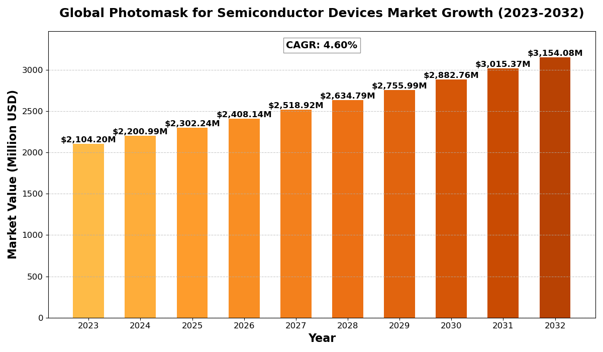
The Global Photomask for Semiconductor Devices Market size was estimated at USD 2104.20 million in 2023 and is projected to reach USD 3154.08 million by 2032, exhibiting a CAGR of 4.60% during the forecast period.
North America Photomask for Semiconductor Devices market size was estimated at USD 592.38 million in 2023, at a CAGR of 3.94% during the forecast period of 2025 through 2032.
- Rising demand for AI, HPC, and 5G chips requiring advanced semiconductor nodes (3nm, 2nm, 1.4nm).
- Increased adoption of EUV lithography, necessitating higher precision photomasks.
- Government initiatives (U.S. CHIPS Act, EU Chips Act, China’s localization efforts) boosting regional photomask production.
Photomask for Semiconductor Devices Key Market Trends :
- Rising Demand for Miniaturized Chips
- Increasing demand for compact and powerful semiconductor devices is driving the adoption of advanced photomasks.
- Advancements in EUV Lithography
- Extreme Ultraviolet (EUV) lithography is gaining momentum, improving efficiency and reducing production costs.
- Growth in AI and IoT Devices
- The rise of artificial intelligence (AI) and the Internet of Things (IoT) is fueling the need for high-performance ICs, boosting the photomask market.
- Increasing Semiconductor Fabrication Facilities
- Governments and private firms are investing in new semiconductor fabs, increasing demand for photomasks.
- Shift Towards 5nm and Below Technology
- As chip manufacturers move towards smaller nodes (5nm and below), photomask technology is evolving to meet precision requirements.
Photomask for Semiconductor Devices Market Regional Analysis :

-
North America:
Strong demand driven by EVs, 5G infrastructure, and renewable energy, with the U.S. leading the market.
-
Europe:
Growth fueled by automotive electrification, renewable energy, and strong regulatory support, with Germany as a key player.
-
Asia-Pacific:
Dominates the market due to large-scale manufacturing in China and Japan, with growing demand from EVs, 5G, and semiconductors.
-
South America:
Emerging market, driven by renewable energy and EV adoption, with Brazil leading growth.
-
Middle East & Africa:
Gradual growth, mainly due to investments in renewable energy and EV infrastructure, with Saudi Arabia and UAE as key contributors.
Photomask for Semiconductor Devices Market Segmentation :
The research report includes specific segments by region (country), manufacturers, Type, and Application. Market segmentation creates subsets of a market based on product type, end-user or application, Geographic, and other factors. By understanding the market segments, the decision-maker can leverage this targeting in the product, sales, and marketing strategies. Market segments can power your product development cycles by informing how you create product offerings for different segments.
Key Company
- Photronics
- Toppan
- DNP
- Hoya
- SK-Electronics
- LG Innotek
- Shenzhen Qingyi Photomask Limited
- Taiwan Mask
- Nippon Filcon
- Compugraphics
- Newway Photomask
Market Segmentation (by Type)
- Quartz Mask
- Soda Mask
- Others
Market Segmentation (by Application)
- IC
- Flat Panel Display
- Touch Industry
- Circuit Board
Drivers
- Growing Demand for Semiconductors: The increasing use of semiconductors in various industries, including automotive and consumer electronics, is driving market growth.
- Expansion of Foundries and Semiconductor Facilities: Leading companies are expanding their production units, increasing demand for photomasks.
- Technological Advancements in Lithography: Innovations in lithography, including EUV and DUV, are enhancing efficiency and reducing costs.
Restraints
- High Initial Investment Costs: The cost of developing advanced photomask technology is significantly high, posing a challenge to market entry.
- Complex Manufacturing Process: Photomask fabrication requires highly sophisticated equipment and expertise, limiting the number of manufacturers.
- Fluctuations in Semiconductor Demand: The cyclic nature of the semiconductor industry affects market stability.
Opportunities
- Growing Demand for 3D Integrated Circuits: The rising adoption of 3D ICs is creating new opportunities for photomask manufacturers.
- Increased Government Support for Semiconductor Manufacturing: Governments worldwide are investing in semiconductor self-sufficiency, creating a favorable market environment.
- Advancements in AI and Quantum Computing: The emergence of AI-driven chip designs and quantum computing is boosting demand for high-precision photomasks.
Challenges
- Stringent Environmental Regulations: Compliance with strict regulations regarding chemical and material usage in photomask production is a challenge.
- Supply Chain Disruptions: Global semiconductor supply chain disruptions impact the availability of raw materials and production schedules.
- Shortage of Skilled Workforce: The photomask industry requires highly skilled professionals, and the current talent gap is a significant hurdle.
Recent Developments in the Photomask Market for Semiconductor Devices :
1. TSMC Expands EUV Photomask Production for 2nm & Beyond
- TSMC has ramped up its EUV photomask production to support 2nm and 1.4nm chip fabrication at its Taiwan and Arizona fabs.
- The company is investing $3 billion in next-gen photomask R&D, improving mask defect detection and repair for high-volume production.
- Apple and NVIDIA are among the first customers adopting TSMC’s advanced photomasks for their next-gen AI and HPC chips.
,January 2025
2. Intel and Samsung Partner on Next-Gen High-NA EUV Photomasks
- Intel and Samsung Foundry announced a strategic partnership to accelerate the development of High-NA EUV photomasks for 1.8nm and smaller nodes.
- High-NA EUV technology, developed with ASML, enables finer patterning and higher yield in semiconductor manufacturing.
- Intel is expected to deploy these photomasks at its Oregon and Ohio fabs, while Samsung integrates them into its Pyeongtaek and Taylor, Texas fabs.
, February 2025
3. Japan’s Dai Nippon Printing (DNP) Invests in Advanced Mask Blanks
- DNP has announced a $500 million investment in next-gen photomask blanks, focusing on low-defect EUV masks and NIL (Nanoimprint Lithography) masks.
- The move comes as Japanese semiconductor manufacturers, including Rapidus and Kioxia, push for local advanced lithography solutions.
- DNP’s new high-purity EUV mask blanks aim to reduce defect rates and improve wafer yield.
, January 2025
5. China’s SMIC Ramps Up DUV Photomask Production for 5nm+ Chips
- SMIC (Semiconductor Manufacturing International Corporation) has increased its deep ultraviolet (DUV) photomask production capacity to support 5nm and 7nm chip manufacturing.
- Due to US export restrictions on EUV lithography tools, SMIC is focusing on DUV-based multi-patterning photomasks to stay competitive.
- Chinese photomask suppliers like Shanghai Micro Electronics Equipment (SMEE) are also developing domestic photomask technology.
, February 2025
6. EU Invests in Photomask Supply Chain to Boost Semiconductor Independence
- The European Commission has allocated €2 billion ($2.2B) in funding to strengthen photomask production within the EU.
- ASML, Zeiss, and Imec are leading initiatives to improve EUV photomask supply chains, reducing reliance on Asian manufacturers.
- This aligns with the European Chips Act, which aims to increase local semiconductor manufacturing.
, February 2025
Key Benefits of This Market Research:
- Industry drivers, restraints, and opportunities covered in the study
- Neutral perspective on the market performance
- Recent industry trends and developments
- Competitive landscape & strategies of key players
- Potential & niche segments and regions exhibiting promising growth covered
- Historical, current, and projected market size, in terms of value
- In-depth analysis of the Photomask for Semiconductor Devices Market
- Overview of the regional outlook of the Photomask for Semiconductor Devices Market:
Key Reasons to Buy this Report:
- Access to date statistics compiled by our researchers. These provide you with historical and forecast data, which is analyzed to tell you why your market is set to change
- This enables you to anticipate market changes to remain ahead of your competitors
- You will be able to copy data from the Excel spreadsheet straight into your marketing plans, business presentations, or other strategic documents
- The concise analysis, clear graph, and table format will enable you to pinpoint the information you require quickly
- Provision of market value data for each segment and sub-segment
- Indicates the region and segment that is expected to witness the fastest growth as well as to dominate the market
- Provides insight into the market through Value Chain
- Market dynamics scenario, along with growth opportunities of the market in the years to come
- 6-month post-sales analyst support
Technological Advancements in Photomasks
EUV (Extreme Ultraviolet) Photomasks
- 2nm and below chip fabrication requires EUV masks with lower defect rates and improved pattern fidelity.
- ASML, Zeiss, TSMC, and Intel are leading High-NA EUV photomask R&D.
- Challenges: EUV masks are expensive ($300,000+ per mask) and require multi-layer deposition for defect reduction.
DUV (Deep Ultraviolet) Photomasks
- Still dominant in 5nm, 7nm, and legacy nodes where EUV adoption is limited.
- SMIC and UMC continue using DUV multi-patterning techniques in China due to EUV restrictions from U.S. sanctions.
Nanoimprint Lithography (NIL) Photomasks
- Canon and Dai Nippon Printing (DNP) are advancing NIL as an alternative to EUV.
- Benefits: Lower cost, simpler processing, and high-resolution patterning without complex optics.
Real-World Examples of Photomask Developments in 2025
1. TSMC’s Advanced EUV Photomasks for 2nm Chips
Real-World Example:
- TSMC has ramped up production of EUV photomasks for its N2 (2nm) process technology, set to power Apple’s M5 chips and NVIDIA’s Blackwell AI GPUs.
- Investment: $3 billion in Taiwan and Arizona fabs to expand photomask production capacity.
- Key Customers: Apple, AMD, Qualcomm, NVIDIA.
- Technological Impact: High-NA EUV photomasks enable denser transistor placement, improving chip power efficiency and performance.
2. Intel & ASML’s High-NA EUV Photomask Collaboration
Real-World Example:
- Intel and ASML have announced the deployment of High-NA EUV photomasks for Intel’s 1.8nm (Intel 18A) process, aimed at HPC (High-Performance Computing) chips.
- Key Innovation: High-NA EUV masks increase resolution by 70%, reducing multi-patterning complexity.
- Impact: First use in Intel’s Ohio fab, expected to rival TSMC’s 2nm technology.
3. Samsung’s EUV Photomask Development for AI Chips
Real-World Example:
- Samsung Foundry is developing next-generation EUV photomasks for 1.4nm node production, targeting AI accelerators and HPC chips.
- Key Customers: Google, Tesla, Meta – all working on custom AI processors.
- Investment: $2.5 billion allocated for EUV photomask R&D in South Korea.
- Strategic Importance: Samsung aims to close the gap with TSMC in leading-edge semiconductor manufacturing.
4. SMIC’s DUV Photomask Expansion in China
Real-World Example:
- SMIC (Semiconductor Manufacturing International Corporation) has increased DUV photomask production to support 5nm and 7nm chip fabrication.
- Reason: Due to U.S. export restrictions, China cannot access ASML’s EUV tools, forcing it to maximize DUV lithography with advanced multi-patterning.
- Government Support: China has invested $1.5 billion in domestic photomask R&D, supporting local suppliers like Shanghai Micro Electronics Equipment (SMEE).
- Impact: Huawei’s Kirin 9000S chip, used in Mate 60 smartphones, was mass-produced with DUV photomasks.
5. Japan’s Dai Nippon Printing (DNP) Investment in EUV Mask Blanks
Real-World Example:
- DNP (Dai Nippon Printing) is increasing production of low-defect EUV mask blanks, essential for 2nm and smaller nodes.
- Investment: $500 million into high-purity EUV mask blanks, enabling lower defect rates in chip manufacturing.
- Partnerships: Supplying Rapidus, Kioxia, and TSMC Japan for Japan’s domestic semiconductor revival.
6. U.S. Photronics Expands Photomask Production for AI Chips
Real-World Example:
- Photronics, a leading photomask supplier, has expanded its U.S. and European operations to meet demand for AI chips and HPC processors.
- Key Customers: AMD, Qualcomm, Intel, and NVIDIA.
- Investment: $350 million in next-gen photomask fabrication facilities.
- Technology Focus: Sub-3nm photomasks with AI-powered defect correction.
7. European Union Invests in Photomask Supply Chain
Real-World Example:
- The European Commission allocated €2 billion ($2.2B) to develop local photomask manufacturing as part of the EU Chips Act.
- Companies Involved: ASML, Zeiss, and Imec are leading initiatives to create EUV photomasks for European semiconductor independence.
- Strategic Impact: Reducing reliance on Taiwan, Japan, and the U.S. for advanced photomask production.
Customization of the Report
In case of any queries or customization requirements, please connect with our sales team, who will ensure that your requirements are met.
FAQs
Q: What are the key driving factors and opportunities in the Photomask for Semiconductor Devices market?
A: The key driving factors include the rising demand for advanced semiconductor devices, growing AI and IoT adoption, and advancements in lithography technologies. Opportunities exist in 3D IC development, increased government investments, and the expansion of semiconductor fabs.
Q: Which region is projected to have the largest market share?
A: Asia-Pacific is expected to hold the largest market share due to the presence of major semiconductor manufacturers, increasing chip demand, and investments in new fabrication facilities.
Q: Who are the top players in the global Photomask for Semiconductor Devices market?
A: Leading players include Photronics, Toppan, DNP, Hoya, SK-Electronics, LG Innotek, Shenzhen Qingyi Photomask Limited, Taiwan Mask, Nippon Filcon, Compugraphics, and Newway Photomask.
Q: What are the latest technological advancements in the industry?
A: Recent advancements include the adoption of EUV lithography, improvements in maskless lithography, and the development of high-precision photomasks for 5nm and below chip nodes.
Q: What is the current size of the global Photomask for Semiconductor Devices market?
A: The market size was estimated at USD 2104.20 million in 2023 and is projected to reach USD 3154.08 million by 2032, growing at a CAGR of 4.60%.

Get Sample Report PDF for Exclusive Insights
Report Sample Includes
- Table of Contents
- List of Tables & Figures
- Charts, Research Methodology, and more...